Semiconductor thin film, semiconductor device and manufacturing method thereof

a technology of semiconductor devices and thin films, applied in non-linear optics, instruments, optics, etc., can solve the problems of insufficient crystallinity of tft active layers for processor circuits or memory circuitry, inability to provide tft active layers, and inability to catch up to strict demands, etc., to achieve enhanced density, reduce the number of possible crystal grain boundaries, and improve the effect of smoothness

Inactive Publication Date: 2006-08-15
SEMICON ENERGY LAB CO LTD
View PDF89 Cites 11 Cited by
  • Summary
  • Abstract
  • Description
  • Claims
  • Application Information

AI Technical Summary

Benefits of technology

[0026]It is a still another object of the invention to provide a semiconductor device capable of offering enhanced performance and reliability without having to make use of single-crystalline semiconductor wafers.
[0033]It should be noted here that the term “mono-domain region” is used to refer to resultant lateral growth crystal region as formed using the semiconductor thin film manufacturing method of the invention, by taking account of the fact that this region is enhanced in crystallinity sufficiently to be regarded as the single crystal in substance. A principal feature of the mono-domain region is that no grain boundaries are found through its entire region, and accordingly, any lattice defects or dislocations are suppressed or eliminated which are otherwise occurred due to presence of transitions and interlayer defects. Another feature is that the mono-domain region avoids inclusion of any metallic elements otherwise acting to badly influence the fundamental characteristics of the semiconductor device.
[0036]The fabrication of such mono-domain region in accordance with the present invention incorporates a unique concept of precisely controlling the location of crystal nucleus by increasing the diameter of respective crystal grains thereby to decrease in number any possible crystal grain boundaries therein.
[0037]The principal approach of the present invention is to extremely smooth the surface of an insulating or dielectric film underlying an amorphous silicon film. To do this, a buffer layer is provided beneath the amorphous silicon film. The buffer layer may be a silicon oxide film as formed by sputtering techniques using an artificial quartz as a target. The composition table of one recommended artificial quartz target used is shown in FIG. 18 for reference. The silicon oxide film thus formed exhibits an enhanced density and increased smoothness, which is free from presence of any possible segregation cites thereon otherwise occurring in the prior art.
[0038]Another key concept of the invention is to pattern the silicon oxide film forming thereon a specific surface configuration of an intended profile pattern, which may include a projection or recess in the surface. In other words, intentional formation of segregation cites of certain metallic element for acceleration or facilitation of crystallization makes it possible to well control the actual locations of crystal nucleus that might take place on the film surface. This may enable formation of grown crystals of any desired sizes at any desired locations, and thus provide great contribution to the semiconductor manufacturers.
[0039]The use of low pressure chemical vapor deposition (CVD) techniques to form the amorphous silicon film on the substrate is also an important feature of the instant invention. As compared to amorphous silicon films formed using plasma CVD techniques, those formed by, the low pressure CVD method offer advantageous characteristics which follow: small in content of hydrogen, more dense in film quality, and less in rate of occurrence of natural crystal nucleus. A decrease in natural nucleus occurrence rate leads to an increase in accuracy of the controllability of crystal nucleus locations.

Problems solved by technology

Unfortunately, the use of such amorphous films is encountered with a problem that where TFTs are required to exhibit higher speeds in operation, amorphous films are incapable of tracing such trend due to its inherently lowered mobility of charge carriers.
Unfortunately, even when the above technique is applied to the manufacture of an active layer of TFTs, resultant TFTs for use in processor circuits or memory circuitry remain insufficient in crystallinity.
As the semiconductor manufacturers are commercially demanded to improve the TFT speed endlessly, employing the above prior art approach to provide the TFT active layer will be unable to catch up the strict demands due to their inherent limitations as to improvements of the crystallinity.
This is because of the fact that the presence or inclusion of such crystal boundaries badly behaves as an energy barrier which can disturb movement or progress of electrons between adjacent crystal grains.
One disadvantage faced with the prior art approach to crystallization is that the presence or formation of a number of segregation cites on the film surface acts to increase the density of crystal nucleus, which in turn undesirably causes the individual crystal grain to disturb the growth of neighboring crystals.
This should result in a decrease in diameter of crystal grain.
However, even this is the case, the positional controllability of crystal nucleus remains very difficult or nearly impossible.
This means that it remains difficult or almost impossible to well control the exact location of segregation cites.
In addition to this, it is shown by the present inventors that any crystalline silicon films fabricated in accordance with the prior art approach discussed previously must contain therein the metallic element that has been utilized during the crystallization process, which disadvantageously serves to deteriorate the stability and reproducibility of semiconductor devices employing the resultant semiconductive film as its active layer or the like.

Method used


Image

  • Semiconductor thin film, semiconductor device and manufacturing method thereof
  • Semiconductor thin film, semiconductor device and manufacturing method thereof
  • Semiconductor thin film, semiconductor device and manufacturing method thereof

Examples


example 1

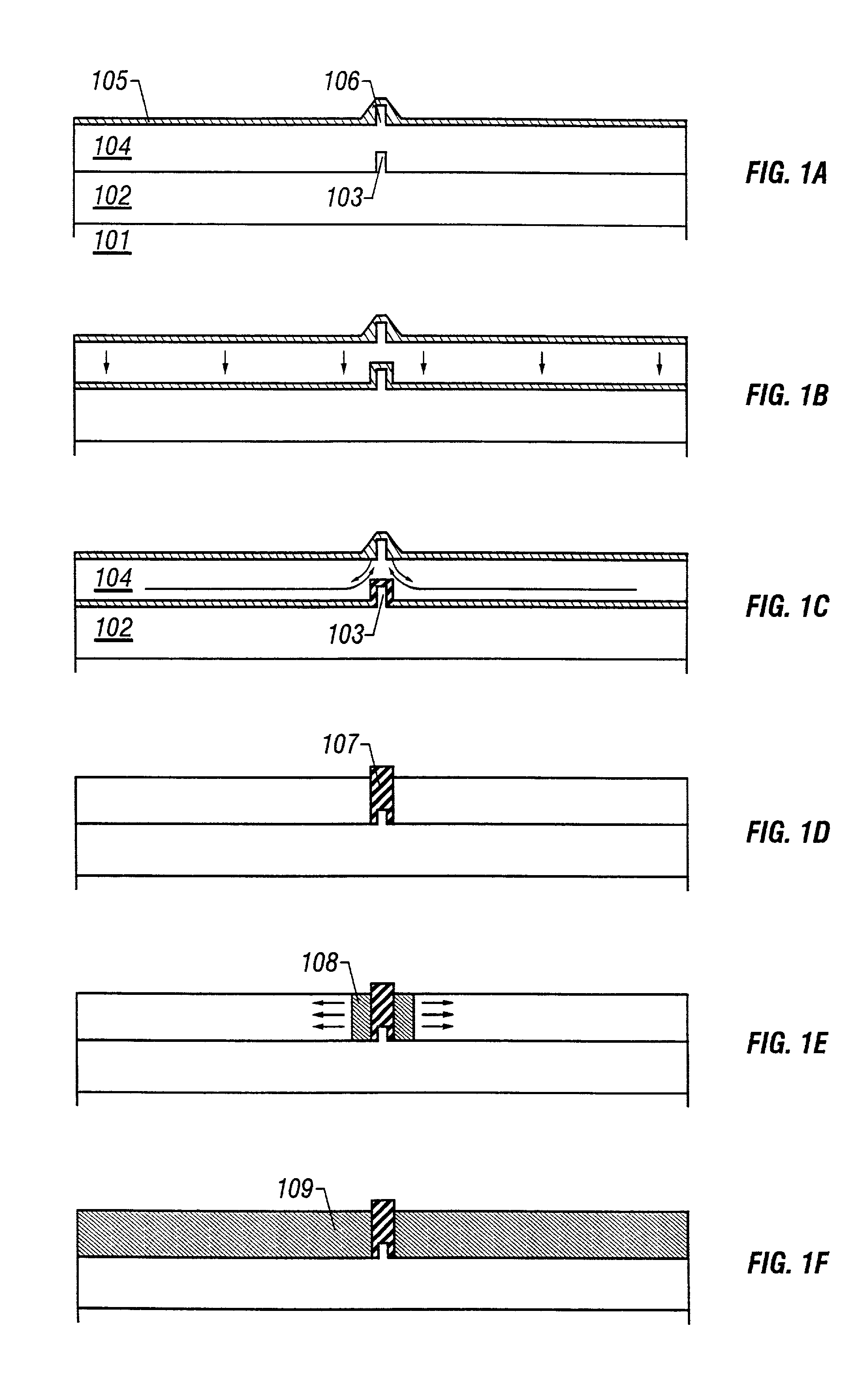
[0058]A fabrication method of a “mono-domain” region which is a key to the invention will be fully described with reference to FIGS. 1A to 1F. See FIG. 1A. This is a diagrammatic depiction (not drawn to scale) of a substrate 101 having an insulating or dielectric surface. The substrate 101 is made of a material of enhanced heat resistance, such as quartz, silicon or the like. As shown, a silicon oxide film 102 is formed by sputtering techniques on substrate 101 with an artificial quartz being as the target. The silicon oxide film 102 exhibits an increased flatness and smoothness on its top surface; for example, any possible surface configuration of film 102 measures 3 nanometers (nm) or less in height and 10 nm or greater in width. This surface configuration will be difficult or nearly impossible to be visually recognized even by use of atomic force microscopy (AFM) measurement schemes.

[0059]After formation of the extra flat silicon oxide film 102, resultant structure is then subjec...

example 2

[0086]A manufacturing method of a TFT structure utilizing the mono-domain of Example 1 is shown in FIGS. 4A to 4E. While this illustrative embodiment will be described herein in connection with a top-gate TFT structure, the invention should not exclusively be limited thereto. One skilled in the art will readily recognize that the method of FIGS. 4A to 4E may alternatively be applicable to formation of a bottom-gate TFT with the gate electrode being replaced by the one which is high in heat resistance.

[0087]As shown in FIG. 4A, a quartz substrate 401 with a silicon oxide film 402 and a “pseudo single-crystalline” mono-domain silicon film 403 being laminated on the surface of substrate 401 in this order. Note that the films 402, 403 may be fabricated using the method shown in FIGS. 1A–1F and 2A–2C. The silicon film 303 has therein a mono-domain region as described previously. Film 403 is patterned by patterning techniques as shown in FIG. 4A. This patterned film 403 will be later used...

example 3

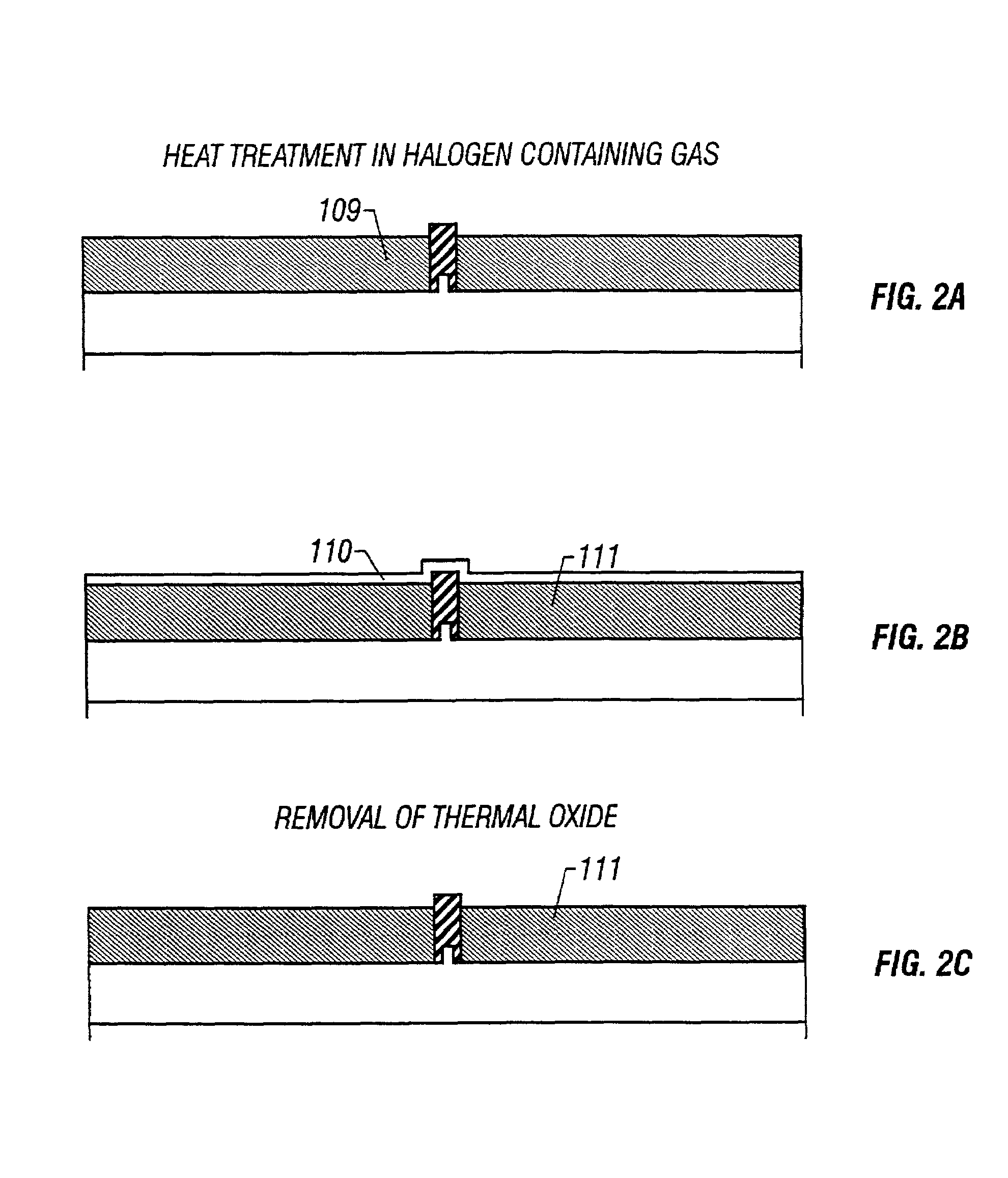
[0098]An explanation will now be given of a significant advantage of the thermal oxidation process in the atmosphere containing halogen elements for formation of the mono-domain region as has been discussed previously in Example 1.

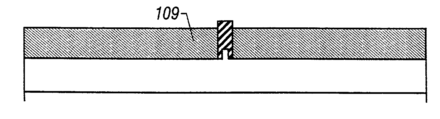
[0099]See FIG. 6. This diagram is a graph showing the relation of vapor pressure of nickel chloride (NiCl2) versus temperature. As shown, since NiCl2 is a sublimative material, Ni in the mono-domain crystalline silicon film 111 of FIG. 2C may exhibit sublimation in nature as soon as it is gettered by chlorine. Resultant nickel chloride compounds will be released from the crystalline silicon film by outdiffusing into the air or by being absorbed by its overlying thermal oxide film. This advantageously serves to enable successful removal of Ni from the silicon film.

[0100]Electrical characteristics of the TFT structure of FIG. 4E will be described with reference to FIG. 5, which demonstrates the relation of gate current (Vg) versus drain voltage (Id) of the T...


PUM

PropertyMeasurementUnit
temperatureaaaaaaaaaa
heightaaaaaaaaaa

Abstract

A semiconductor device includes a substrate having an insulating film on its surface, and ac active layer made of a semiconductive thin film on the substrate surface. The thin film contains a mono-domain region formed of multiple columnar and / or needle-like crystals parallel to the substrate surface without including crystal boundaries therein, allowing the active layer to consist of the mono-domain region only. The insulating film underlying the active layer has a specific surface configuration of an intended pattern in profile, including projections or recesses. To fabricate the active layer, form a silicon oxide film by sputtering on the substrate. Pattern the silicon oxide film providing the surface configuration. Form an amorphous silicon film by low pressure CVD on the silicon oxide film. Retain in the silicon oxide film and / or the amorphous silicon film certain metallic element for acceleration of silicon film to a crystalline silicon film. Then, perform a second heat treatment in the halogen atmosphere forming on the crystalline silicon film a thermal oxide film containing halogen, whereby the crystalline silicon film alters to a mono-domain region.

Description

[0001]This application is a continuation of U.S. application Ser. No. 09 / 571,500, filed May 15, 2000 now U.S. Pat. No. 6,323,072, which is a divisional of U.S. application Ser. No. 08 / 802,276, filed Feb. 19, 1997 now U.S. Pat. No. 6,093,937.BACKGROUND OF THE INVENTION[0002]1. Field of the Invention[0003]The present invention relates generally to semiconductor devices, and more particularly to semiconductor devices having a semiconductive thin film as its active layer and the manufacturing method thereof. The invention also relates to thin film semiconductor transistors with an active layer made of crystalline silicon films.[0004]2. Description of the Prior Art[0005]In the recent years semiconductor thin-film transistor (TFT) devices are becoming more widely used in the manufacture of electronic parts or components, particularly reduced-thickness display devices and digital integrated circuit (IC) packages, as the speed and cost advantages of these devices increase. As such electroni...

Claims


Application Information

Patent Timeline
Patent Type & Authority Patents(United States)
IPC IPC(8): H01L29/04G02F1/1362H01L21/20H01L21/336H01L21/77H01L21/84H01L27/108H01L27/11H01L27/12
CPCG02F1/13454H01L27/10805H01L27/10873H01L27/11H01L27/12H01L27/1203H01L27/1277H01L27/1281H01L27/1296H01L29/04H01L27/1108H01L21/02532H01L21/02672H01L29/66757H10B12/30H10B12/05H10B10/00H10B10/125H01L29/786
Inventor YAMAZAKI, SHUNPEIKOYAMA, JUNMIYANAGA, AKIHARUFUKUNAGA, TAKESHI
Owner SEMICON ENERGY LAB CO LTD
Why Eureka
Try Eureka