Semiconductor device and method of manufacturing the same

a semiconductor and semiconductor technology, applied in semiconductor devices, electrical devices, transistors, etc., can solve the problems of poor heat resistance of glass substrates, easy thermal deformation, and sudden attention of continuous wave laser beams, and achieve high current driver performan

Inactive Publication Date: 2006-09-12
SEMICON ENERGY LAB CO LTD
View PDF43 Cites 50 Cited by
  • Summary
  • Abstract
  • Description
  • Claims
  • Application Information

AI Technical Summary

Benefits of technology

[0027]In view of the aforementioned problems, an object of the present invention is to provide a semiconductor device structured by a high speed semiconductor element having high current driver performance, in which a crystalline semiconductor film is formed on an insulating surface, and the crystalline semiconductor film has as few crystal grain boundaries and crystal subboundaries as possible intersecting at least with a channel length direction.

Problems solved by technology

A glass substrate is inferior in heat resistance and is easily subjected to thermal deformation.
As a result, continuous wave laser beams are now suddenly attracting attention.
The position and size of the crystal grains are random, and it is difficult to specify the crystal grain position and size when forming a crystalline semiconductor film.
However, it is nearly impossible to form an amorphous silicon film, in which grain boundaries do not exist, by using a laser annealing method.
It has therefore not been possible to date to obtain characteristics equivalent to those of a MOS transistor, which is manufactured on a single crystal silicon substrate, in a TFT that uses a crystalline silicon film crystallized by employing laser annealing.
A step on the base like that of a known graphoepitaxy technique is utilized, and therefore crystals grow along the step, but the step which remains in the surface of the formed single crystal semiconductor film is considered to be a problem.
In addition, a single crystal semiconductor film cannot be formed on a glass substrate having a relatively low distortion point by using graphoepitaxy.
In any case, it has not been possible to form a crystalline semiconductor film in which semiconductor volumetric contraction caused by crystallization, defects due to thermal stresses with the base, lattice mismatching, or the like, crystal grain boundaries, and subboundaries do not exist.
Except a bonded SOI (silicon on insulator), it has not been possible to obtain quality equivalent to that of a MOS transistor formed on a single crystal substrate, in a crystalline semiconductor film that is formed on an insulating surface and then crystallized or recrystallized.

Method used


Image

  • Semiconductor device and method of manufacturing the same
  • Semiconductor device and method of manufacturing the same
  • Semiconductor device and method of manufacturing the same

Examples


embodiment mode 1

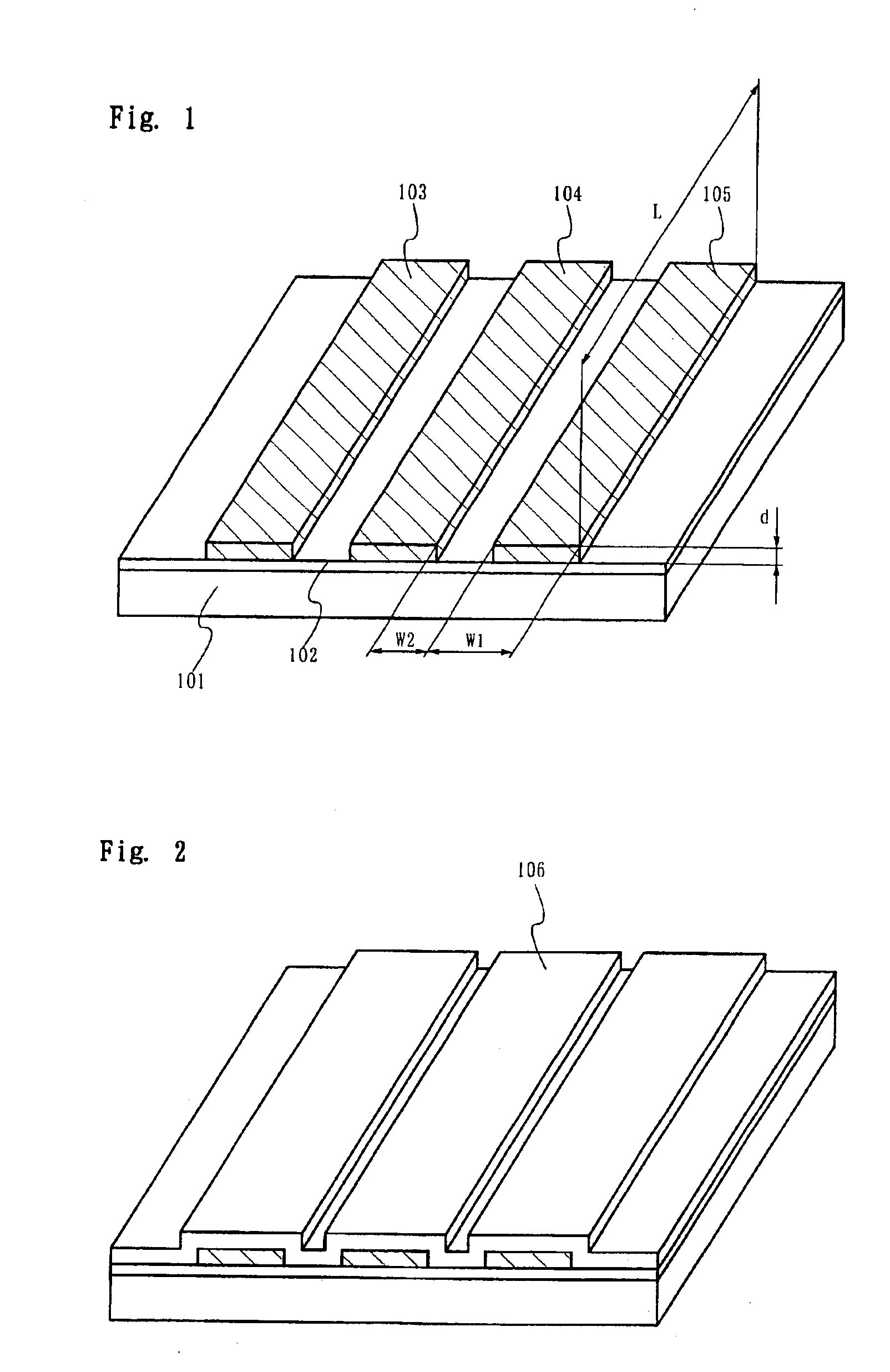
[0129]An embodiment mode of the present invention is explained below with reference to the figures. A perspective view shown in FIG. 1 shows an embodiment in which a first insulating film 102, and second insulating films 103 to 105 that are patterned into stripe shapes, are formed on a substrate 101. Three stripe shape patterns are shown here for the second insulating films, but of course there are not limitations placed on the number of stripe shape patterns. The substrate can apply a commercially available non-alkaline glass substrate, a quartz substrate, a sapphire substrate, a single crystal or a polycrystalline semiconductor substrate whose surface is covered by an insulating film, or a metal substrate whose surface is covered by an insulating film.

[0130]The A width W1 of the second insulating films formed in stripe shapes is set from 0.1 to 10 μm (preferably from 0.5 to 1 μm), a gap W2 between adjacent second insulating films is set from 0.1 to 5 μm (preferably from 0.5 to 1 μ...

example 1

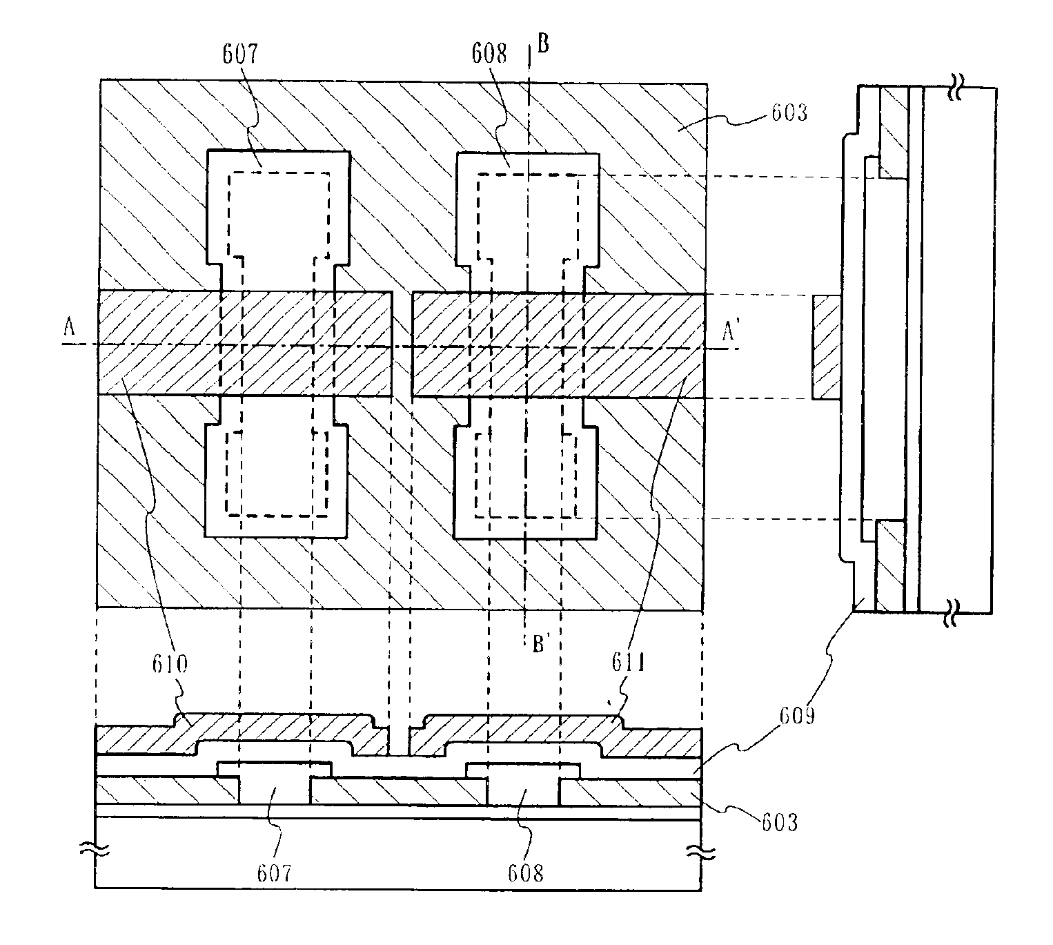
[0170]This Example shows an example of manufacturing a TFT in which a crystalline silicon film is formed on a base insulating film having an opening portion, and a channel formation region is disposed in a filled region filling the opening portion.

[0171]A first insulating film 602 is formed by silicon nitride film with a thickness of a 100 nm on a glass substrate 601 in FIGS. 7A to 7C. A silicon oxide film is formed on the first insulating film 602, and second insulating films 603 having a rectangular shape pattern are formed by photoetching. The silicon oxide film is deposited to a thickness of 150 nm by using plasma CVD with a mixture of TEOS and O2, and by discharging at a high frequency (13.56 MHz) electric power density of 0.6 W / cm2 with a reaction pressure of 40 Pa and a substrate temperature of 400° C. Opening portions 604a and 604b are then formed by etching.

[0172]Note that FIG. 7A is an upper surface diagram, FIG. 7B is a longitudinal cross sectional diagram corresponding t...

example 2

[0179]Example 2 shows a structure formed by processes that are similar to those of Example 1, but as shown by FIGS. 12A to 12C, the opening portions formed in the second insulating films 603 are formed in long, thin strip regions and regions that are connected to the long, thin strip regions. As island-like semiconductor region 620 is formed by a crystalline silicon film in alignment with the opening portion 604c, and a single gate, multi-channel TFT can be completed by forming a gate insulating film 621 and a gate electrode 622.


PUM


Abstract

An objective is to provide a method of manufacturing a semiconductor device, and a semiconductor device manufactured by using the manufacturing method, in which a laser crystallization method is used that is capable of preventing the formation of grain boundaries in TFT channel formation regions, and is capable of preventing conspicuous drops in TFT mobility, reduction in the ON current, and increases in the OFF current, all due to grain boundaries. Depressions and projections with stripe shape or rectangular shape are formed. Continuous wave laser light is then irradiated to a semiconductor film formed on an insulating film along the depressions and projections with stripe shape of the insulating film, or along a longitudinal axis direction or a transverse axis direction of the rectangular shape. Note that although it is most preferable to use continuous wave laser light at this point, pulse wave laser light may also be used.

Description

BACKGROUND OF THE INVENTION[0001]1. Field of the Invention[0002]The present invention relates to a semiconductor device formed by using a semiconductor film having a crystalline structure, and to a method of manufacturing the semiconductor device. The present invention also relates to a semiconductor device containing a field effect transistor, in particular, a thin film transistor, in which an island-like semiconductor region containing a channel formation region is formed by a crystalline semiconductor film formed on an insulating surface, and to a method of manufacturing the semiconductor device.[0003]2. Description of the Related Art[0004]In recent years, a technique of forming a TFT on a substrate has greatly progressed, and its application and development for active matrix semiconductor display devices have been advanced. In particular, since a TFT using a polycrystalline semiconductor film has higher field-effect mobility (also referred to as mobility) than a TFT using a conv...

Claims


Application Information

Patent Timeline
Patent Type & Authority Patents(United States)
IPC IPC(8): H01L21/50H01L21/336H01L21/77H01L21/84H01L27/12H01L29/786
CPCH01L27/12H01L29/66757H01L27/1281H01L29/78675H01L29/78696H01L29/78621H01L29/786
Inventor ISOBE, ATSUOYAMAZAKI, SHUNPEIKOKUBO, CHIHOTANAKA, KOICHIROSHIMOMURA, AKIHISAARAO, TATSUYAMIYAIRI, HIDEKAZUAKIBA, MAI
Owner SEMICON ENERGY LAB CO LTD
Why Eureka
Try Eureka