Vertical MOSFET SRAM cell

Inactive Publication Date: 2006-11-21
IBM CORP
View PDF10 Cites 50 Cited by
  • Summary
  • Abstract
  • Description
  • Claims
  • Application Information

AI Technical Summary

Benefits of technology

[0021]In accordance with this invention an advantage is that

Problems solved by technology

We believe that there is a problem with a structure with individual floating body devices the components of the cross coupled inverters of an SRAM circuit.
The problem is that with individual floating body devices the devices suffer from Vt mismatch, which means that the values of matched pull-up transistor pairs and matched pull-down transistor pairs will float to divergent Vt values due to body charging.
In addition to potential loss of data due to errors caused by highly divergent Vt values, in less serious cases of Vt mismatch the result will be a compromise in the sensitivity of the cell.
When the Vt values of the matched transistor pairs diverge, there is a significant risk of loss of data.
The alternative of providing external body contacts is undesirable in that valuable surface area of the SRAM structure will be required to locate the contacts.
Often that none-obvious combination of materials and process steps may results in drawbacks and/or incompatibility with other structures.
The intrinsic polysilicon is not a good insulator material.
As referred to herein above, this produces a large Vt mismatch.
This mismatch can slow down sensing (i.e., a slower set pulse is required) or it results in a complete failure

Method used


Image

  • Vertical MOSFET SRAM cell
  • Vertical MOSFET SRAM cell
  • Vertical MOSFET SRAM cell

Examples


Embodiment Construction

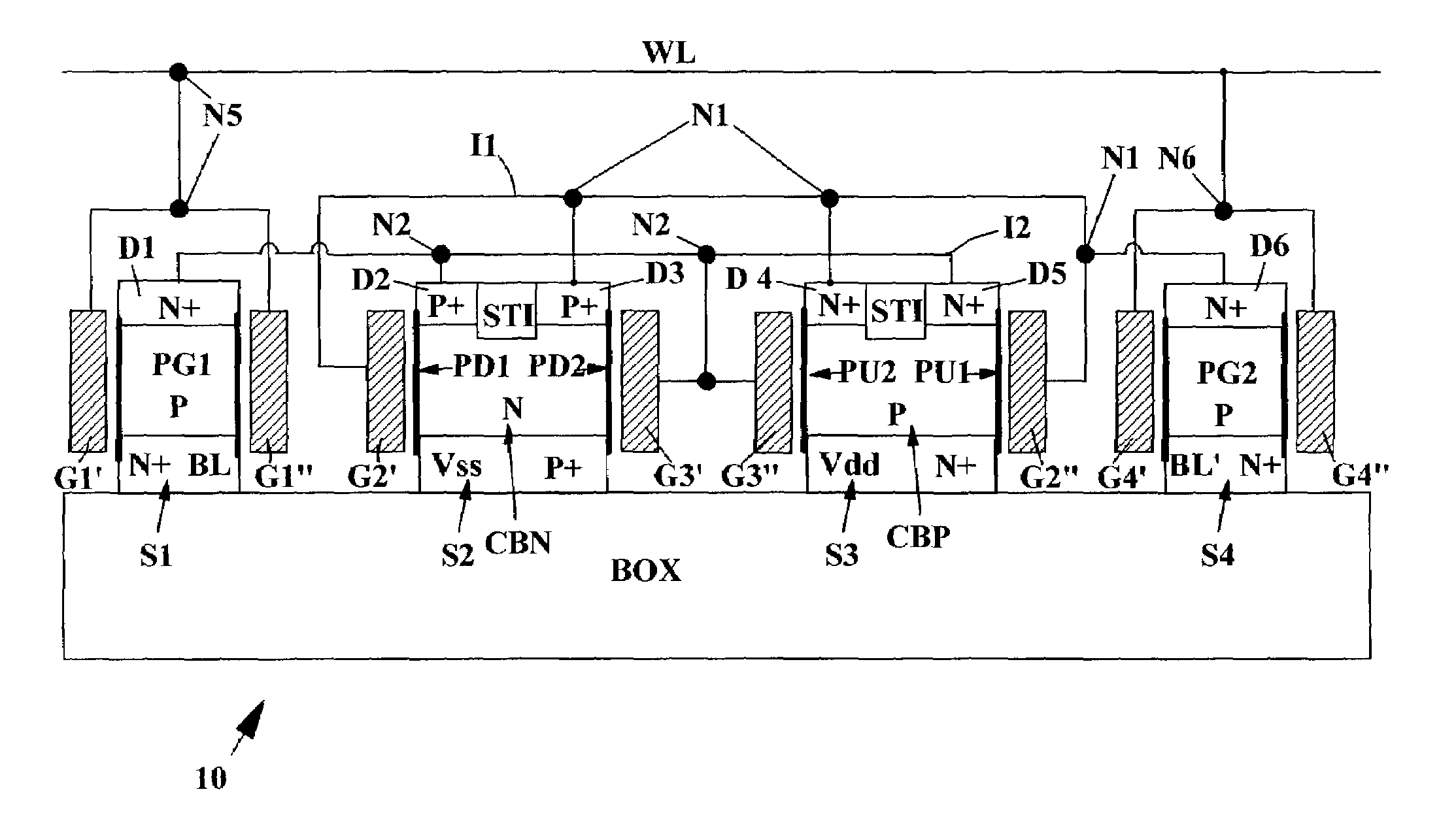
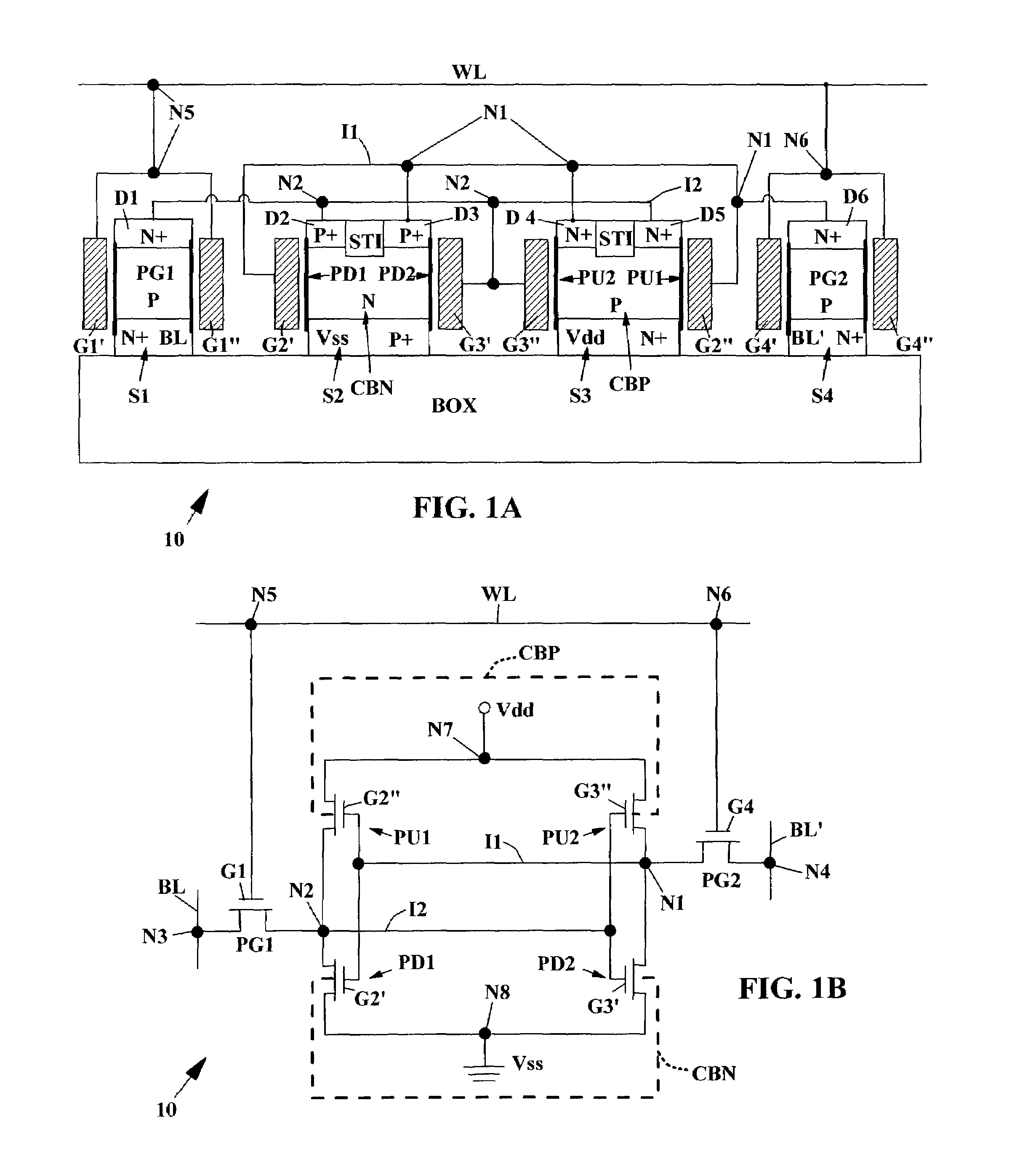
[0044]FIG. 1A illustrates a structure made in accordance with the method of this invention comprising an SRAM cell circuit 10 including a cross-coupled latch device solely comprising vertical channel MOSFETs (Metal Oxide Semiconductor Field Effect Transistors). The entire cell circuit 10, including the pass gate transistors PG1 / PG2 and the cross-coupled inverters formed by four MOSFET transistors PD1, PD2, PU1 and PU2, occupies an area (including isolation) of 112F2. Interconnection of the drains D2 / D5 and D3 / D4 of the cross-coupled pairs of MOSFET transistors PD1, PD2, PU1 and PU2 in the SRAM circuit is provided by lower level wiring M0 and studs which are borderless to the gate conductors. The next level of wiring M1, which is borderless to the lower level wiring M0, is used to cross-couple the inverters PD1, PD2, PU1 and PU2 and to connect their outputs to the pass gate MOSFETs PG1 and PG2 of the SRAM cell circuit 10.

[0045]However, the size of the SRAM device can be reduced to be...


PUM


Abstract

A method of forming an SRAM cell device includes the following steps. Form pass gate FET transistors and form a pair of vertical pull-down FET transistors with a first common body and a first common source in a silicon layer patterned into parallel islands formed on a planar insulator. Etch down through upper diffusions between cross-coupled inverter FET transistors to form pull-down isolation spaces bisecting the upper strata of pull-up and pull-down drain regions of the pair of vertical pull-down FET transistors, with the isolation spaces reaching down to the common body strata. Form a pair of vertical pull-up FET transistors with a second common body and a second common drain. Then, connect the FET transistors to form an SRAM cell.

Description

BACKGROUND OF THE INVENTION[0001]1. Field of the Invention[0002]This invention relates to MOSFET SRAM cells and more particularly to a method of manufacturing a Vertical MOSFET SRAM cell and the structure provided thereby.[0003]2. Description of Related Art[0004]Use of vertical channel MOSFETs enables precise control of channel length, for high performance applications.[0005]U.S. Pat. No. 6,477,080 of Noble for “Circuits and Methods for a Static Random Access Memory Using Vertical Transistors” describes a vertical SRAM device with floating bodies of the FET devices in the SRAM circuit. The patent also states as follows:[0006]“The n-channel and p-channel transistors of memory cell . . . have gates that are formed of n+ and p+ polysilicon, respectively. The polysilicon gates in an inverter are coupled together with a gate contact that is formed of a refractory metal so as to provide a dual work function feature for desired surface channel characteristics in each transistor in the inve...

Claims


Application Information

Patent Timeline
IPC IPC(8): H01L21/00G11C11/412H01L21/8244H01L21/84H01L27/11H01L27/12
CPCG11C11/412H01L21/84H01L27/11H01L27/1104H01L27/1203H10B10/00H10B10/12
Inventor HSU, LOUIS L.GLUSCHENKOV, OLEGMANDELMAN, JACK A.RADENS, CARL J.
Owner IBM CORP
Why Eureka
Try Eureka