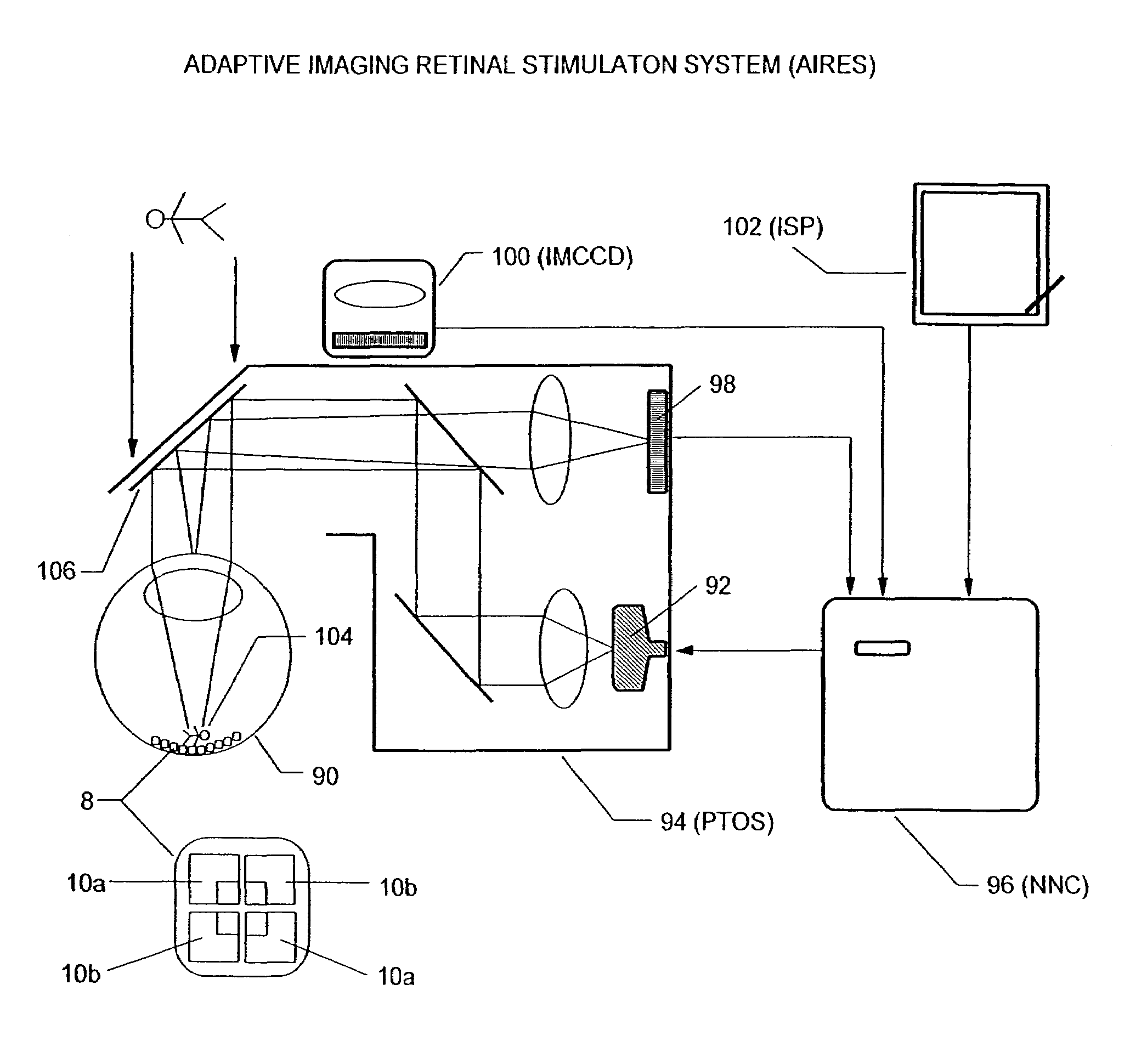
Multi-phasic microphotodiode retinal implant and adaptive imaging retinal stimulation system
- Summary
- Abstract
- Description
- Claims
- Application Information
AI Technical Summary
Benefits of technology
Problems solved by technology
Method used
Image
Examples
second embodiment
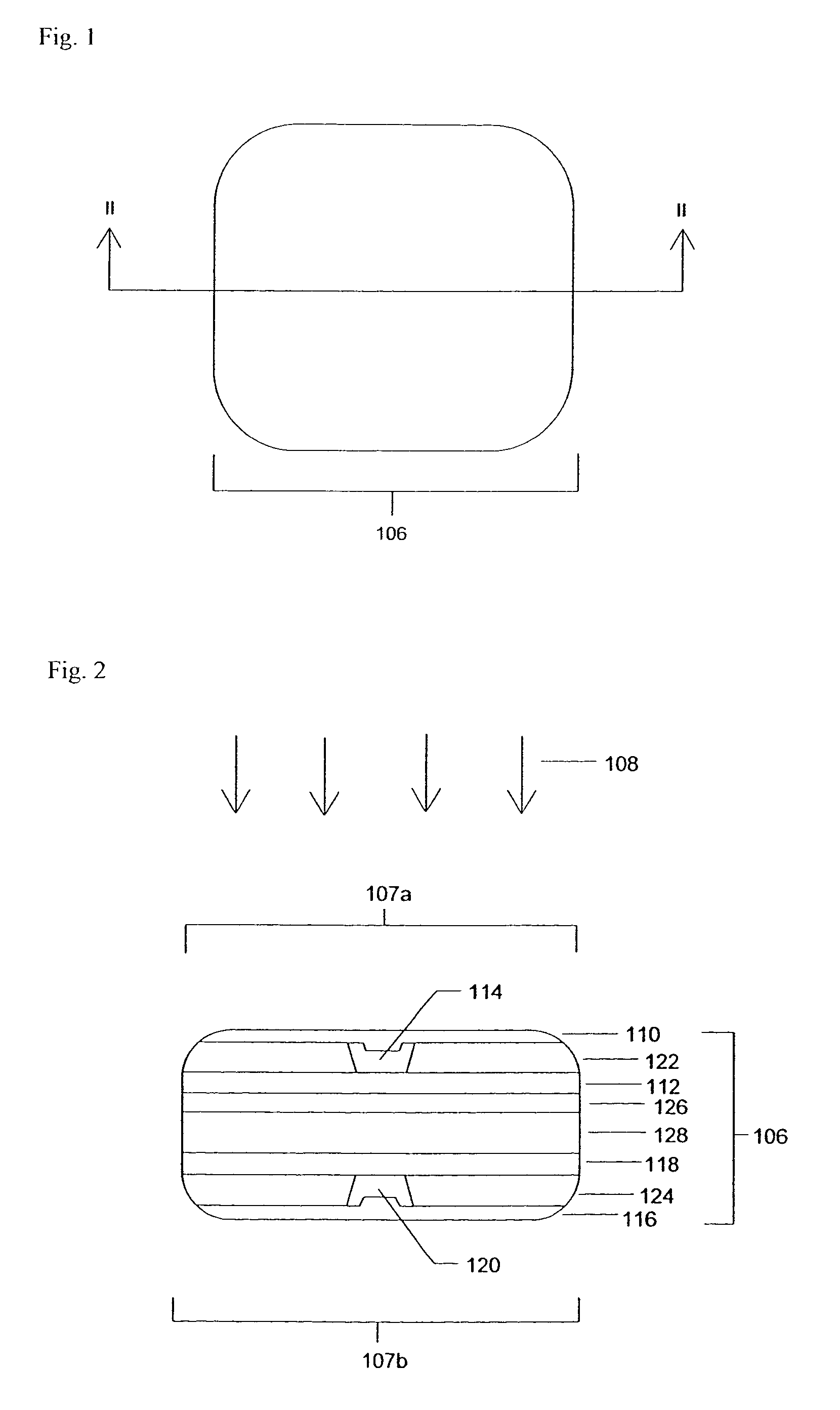
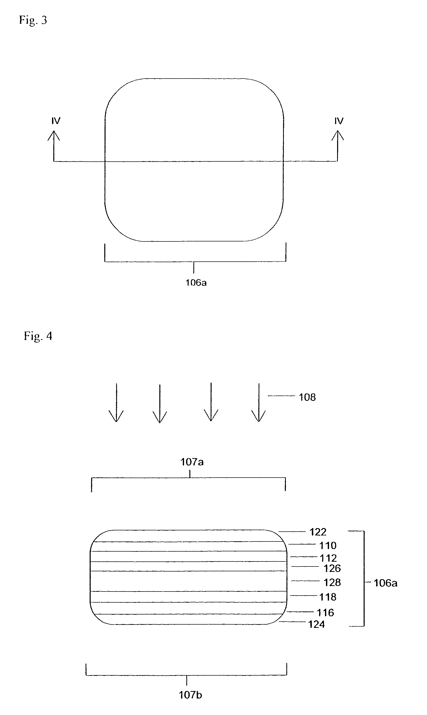
[0050]In this invention (MMRI-E) (FIG. 3–4), the MMRIs of FIGS. 1–2 are fabricated so that the polysilicon layer 110 is sandwiched between the multi-layer dielectric visible light filter layer 122 and the P+ layer 112, and the polysilicon layer 116 is sandwiched between the multi-layer dielectric IR filter layer 124 and the N+ layer 124. The aluminum contact pads 114 and 120 of FIGS. 1–2 are not be needed in this embodiment. This embodiment results in MMRI-Es which predominately stimulated retinal cells adjacent to the MMRI-Es rather than on top of the MMRI-Es. This second embodiment is used in those patients where side simulation will induce better vision than top stimulation. The remaining layers of the intrinsic layer 126, and the N-type silicon substrate layer 128, the P-side 107a, and the N-side 107b are unchanged.
[0051]FIG. 5, A through L illustrates the manufacturing steps of the preferred MMRIs. As shown in FIG. 5A, a 3″ float zone 1-0-0 N-type silicon wafer (140) at 200 to ...
third embodiment
[0053]FIGS. 6–7 illustrate the layered microarchitecture of the artificial retina device of this invention, designated at (8), and is referred to for convenience as a MMRI-4 to distinguish it from other embodiments of this invention. MMRI-4 (8) forms the shape of a flattened cube with rounded corners and edges, and is sized in microscopic dimensions. It is comprised of four microphotodiode subunits (10a×2 and 10b×2). Each microphotodiode subunit (10a or 10b) of the MMRI-4 (8) may be a PiN or NiP device, depending upon which of its photosensitive surfaces is oriented toward light (12). For example, as shown in FIG. 7, the near left microphotodiode (10a) is behaving as a PiN subunit, because the P+ tub (14) is facing incident light (12). In contrast, the near right microphotodiode (10b) is behaving as a NiP subunit because its N+ tub (18) is facing incident light (12). It can be readily appreciated, that if the MMRI-4 (8) is flipped over, the microphotodiode subunit (10a) will have it...
fourth embodiment
[0057]FIGS. 8–9 illustrate the layered microarchitecture of the artificial retina device of this invention, designated at (8a), and is referred to for convenience as a MMRI-4E to distinguish it-from other embodiments of this invention. MMRI-4E (8a) forms the shape of a flattened cube with rounded corners and edges, and is sized in microscopic dimensions. It is comprised of four microphotodiode subunits (10a×2 and 10b×2). Each microphotodiode subunit (10a or 10b) of the MMRI-4E (8a) may be a PiN or NiP device, depending upon which of its photosensitive surfaces is oriented toward light (12). For example, as shown in FIG. 9, the near left microphotodiode (10a) is behaving as a PiN subunit, because the P+ tub (14) is facing incident light (12). In contrast, the near right microphotodiode (10b) is behaving as a NiP subunit because its N+ tub (18) is facing incident light (12). It can be readily appreciated, that if the MMRI-4E (8a) is flipped over, the microphotodiode subunit (10a) will...
PUM
 Abstract
Description
Claims
Application Information


