Methods of forming boron carbo-nitride layers for integrated circuit devices
- Summary
- Abstract
- Description
- Claims
- Application Information
AI Technical Summary
Benefits of technology
Problems solved by technology
Method used
Image

Examples
example 1
Creation of BCN Films
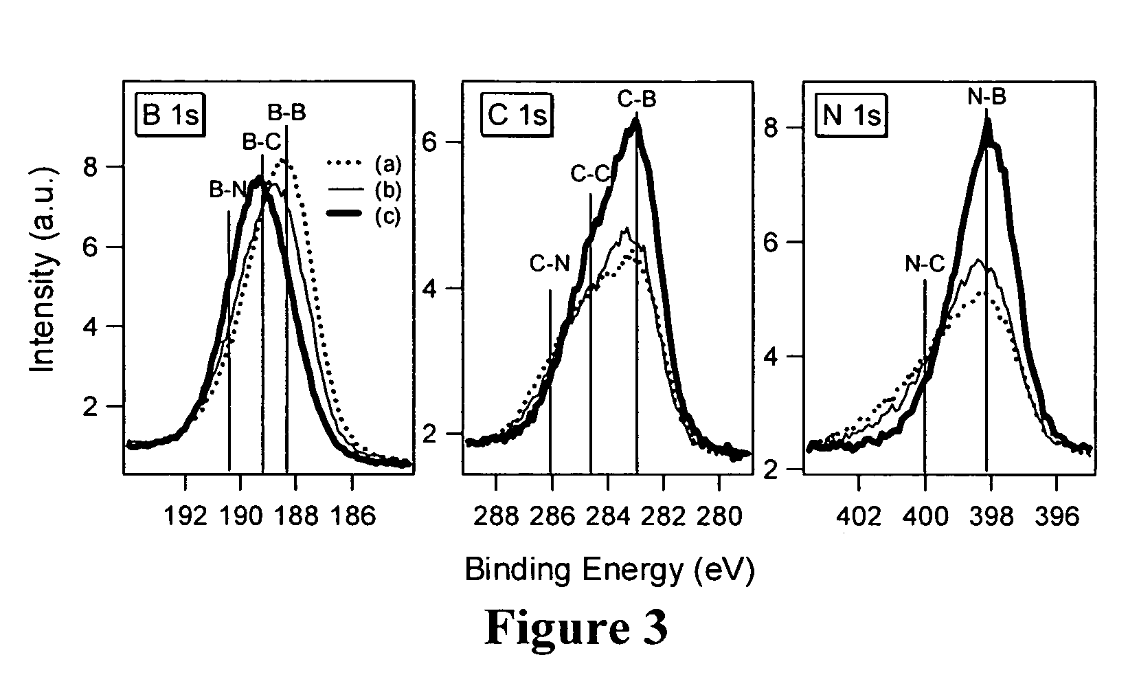
[0032]Films were deposited by thermal CVD in a film deposition facility consisting of a load lock, sample transfer system, CVD growth chamber, and analysis chamber equipped with X-ray photoelectron spectroscopy (XPS) as described elsewhere. Dimethylamine borane complex [NH(CH3)2:BH3] (DMAB) from Strem Chemicals, Inc. (97% purity) was delivered to the reactor from a stainless steel bubbler containing approximately 50 g of the precursor and held at 27° C. DMAB is a white crystalline solid with a melting point of 36° C. and vapor pressure of 1.5 mTorr at 60° C. DMAB vapor was carried to the reactor by ultra high purity (UHP, 99.999%) argon carrier gas delivered through a mass flow controller. UHP ammonia was also delivered through a mass flow controller. Reaction gas streams were mixed at the reactor doser approximately 4 cm above the substrate surface to minimize gas phase reactions while allowing uniform gas mixing at the substrate surface.
[0033]The films were de...
example 2
The Effect of Temperature on Film Deposition and Properties
[0036]Films were deposited by CVD on thermal SiO2 over a temperature range from 360° C. to 500° C. at 1 Torr to investigate the effect of substrate temperature on film deposition and properties. The argon carrier gas flow rate was held constant through the DMAB bubbler at 10 sccm. Table I shows the film composition measured in-situ using XPS for different deposition temperatures and the resulting dielectric constant. As the temperature increased, the boron concentration decreased while both the nitrogen and carbon increased. Oxygen was under 3 atom (at) % in the films, decreasing with temperature. Films deposited had a stoichiometric composition of BC0.26N0.15 at 360° C., BC0.37N0.17 at 420° C., and BC0.37N0.25 at 500° C. The deposition temperature affected the film deposition rate. The deposition rate was 0.34 nm / min at 360° C., 1.5 nm / min at 420° C., and 4.0 nm / min at 500° C. Table I shows the dependence of the dielectric ...
example 3
The Effect of Ammonia on Film Deposition and Properties
[0040]Films were deposited by CVD on thermal SiO2 at 360° C. and 1 Torr to study the effect of NH3 as a reaction gas on films deposited using DMAB. The argon carrier gas flow rate was again held constant at 10 sccm through the DMAB bubbler, with the ammonia flow rate varied from 0 to 10 sccm. Table II shows the resulting film composition and the dielectric constant for the films deposited with varying ammonia flow rate. As the ammonia flow rate increased the nitrogen content increased in the film, displacing carbon and some boron in the film. The nitrogen to boron ratio increased from 0.15 with no ammonia flow to 0.58 with 10 sccm ammonia. At 10 sccm ammonia, both the carbon and oxygen in the film decreased to less than 3%. The approximate deposition rate increased to 0.60 nm / min at the lower ammonia flow rates (0.4 and 1.0 sccm) compared to 0.34 nm / min for no ammonia flow, and decreased to 0.49 nm / min at 10 sccm. Ammonia flow r...
PUM
 Abstract
Description
Claims
Application Information
 - R&D Engineer
- R&D Manager
- IP Professional
- Industry Leading Data Capabilities
- Powerful AI technology
- Patent DNA Extraction
Browse by: Latest US Patents, China's latest patents, Technical Efficacy Thesaurus, Application Domain, Technology Topic.
© 2024 PatSnap. All rights reserved.Legal|Privacy policy|Modern Slavery Act Transparency Statement|Sitemap