Method to plasma deposit on organic polymer dielectric film

Active Publication Date: 2007-01-16
TAIWAN SEMICON MFG CO LTD
View PDF16 Cites 352 Cited by
  • Summary
  • Abstract
  • Description
  • Claims
  • Application Information

AI Technical Summary

Benefits of technology

[0034]An optimized PENLD process can perform both continuous and plasma assisted layer without many changes. A typical PENLD process deposits about 10–20 angstrom thermal layer, and then uses plasma species such as nitrogen or hydrogen to densify the deposited layer. In a typical PENLD process, the nucleation time varied depending on the substrates, therefore the first few layers might not received 10–20 angstrom thickness.

Problems solved by technology

The conductivity of interconnects is reduced as the surface area of interconnects is reduced, and the resulting increase in interconnect resistivity has become an obstacle in IC design.
Conductors having high resistivity create conduction paths with high impedance and large propagation delays.
These problems result in unreliable signal timing, unreliable voltage levels, and lengthy signal delays between components in the IC.
Propagation discontinuities also result from intersecting conduction surfaces that are poorly connected, or from the joining of conductors having highly different resistivity characteristics.
However, there have been problems associated with the use of copper in IC processing.
Copper poisons the active area of silicon devices, creating unpredictable responses.
Precursor by-products (products formed as the precursor decomposes that do not participate in the reactions) and reaction by-products (products formed from the reaction that are not deposited on the selected surfaces) are often volatile and being exhausted away.
The porous low-k dielectrics present a significant integration problem such as low mechanical strength, poor dimensional stability, poor temperature stability, high moisture absorption, permeation, poor adhesio

Method used


Image

  • Method to plasma deposit on organic polymer dielectric film
  • Method to plasma deposit on organic polymer dielectric film
  • Method to plasma deposit on organic polymer dielectric film

Examples


first embodiment

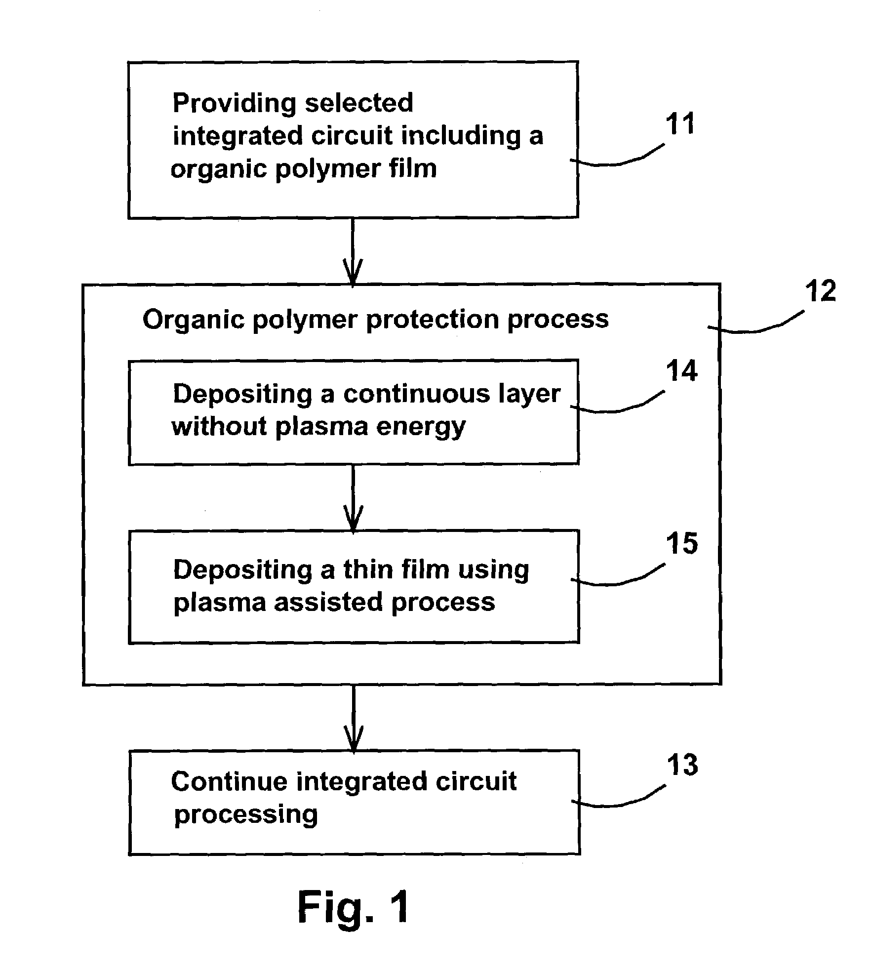
[0044]FIG. 1 is a flowchart showing the steps in the method to protect the organic polymer dielectric underlayer. Step 11 provides the selected integrated circuit including an organic polymer dielectric film. Step 12 shows the current invention organic polymer protection process comprising 2 steps: step 14 and step 15. Step 14 provides the deposition of a continuous film using non plasma process in order to not damage the organic polymer dielectric film and to protect the organic polymer dielectric film during the plasma exposure of the next step. Then step 15 provides the plasma assisted deposition of a thin film on top of the continuous film. Step 13 provides the rest of the integrated circuit processing such as interconnect and passivation. To not exposing the organic polymer dielectric film to an ambient containing energetic plasma excited species, step 14 provides a protection layer. The deposition step 14 and the deposition step 15 can be processed in the same process chamber,...

second embodiment

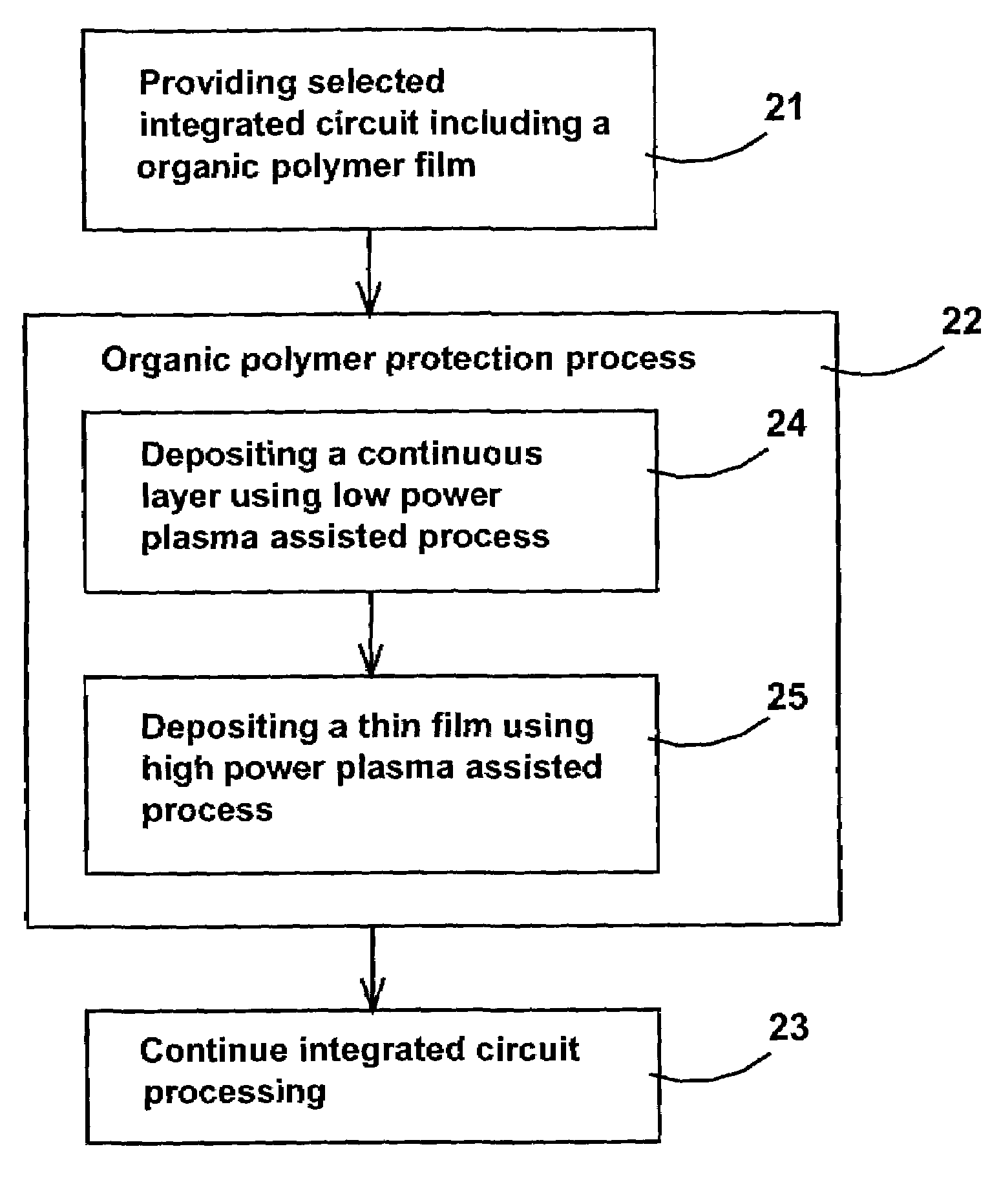
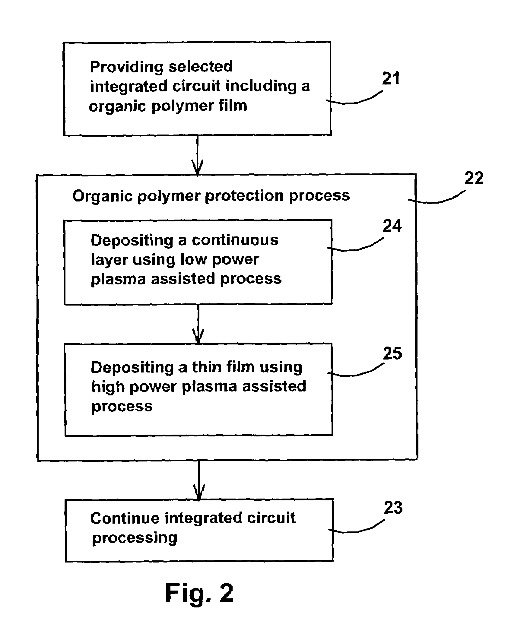
[0045]FIG. 2 is a flowchart showing the steps in the method to protect the organic polymer dielectric underlayer. Step 21 provides the selected integrated circuit. Step 22 shows the current invention organic polymer protection process comprising 2 steps: step 24, 26 and step 25. Step 24 provides the deposition of a continuous film using low power plasma process in order to not damage the organic polymer dielectric film and to protect the organic polymer dielectric film during the plasma exposure of the next step. Then step 25 provides a high power plasma assisted deposition of a thin film on top of the continuous film. Step 23 provides the rest of the integrated circuit processing such as interconnect and passivation. Typically, the deposition of the continuous film and the deposition of the impermeable film are occurred in the same process chamber if the materials in these 2 films are similar, such as TiN with different levels of plasma energies. The depositions can occur in 2 sepa...


PUM

PropertyMeasurementUnit
Plasma poweraaaaaaaaaa

Abstract

A method for protecting an organic polymer underlayer during a plasma assisted process of depositing a subsequent film on the organic polymer underlayer is disclosed. The method provides the deposition of a protective continuous layer using organic polymer damage-free technique in order to not damage the organic polymer underlayer and to protect the organic polymer underlayer during the plasma assisted process of depositing a subsequent film. The organic polymer damage-free technique is a non-plasma process, using only thermal energy and chemical reactions to deposit the continuous layer. The organic polymer damage-free technique can also be a plasma assisted process using a reduced plasma power low enough in order to not damage the organic polymer underlayer. This method is applicable to many organic polymer underlayers such as organic polymer is aromatic hydrocarbon, polytetrafluoroehtylene (PTFE), parylene, benzocyclobutene-based polymers (BCB), polyimide, fluorinated polyimide, fluorocarbon-based polymers, poly(arylene ether)-based polymers (PAE), cyclohexanone-based polymers, and to many plasma assisted deposition processes such as plasma enhanced CVD deposition, plasma enhanced ALD deposition and plasma enhanced NLD deposition of silicon dioxide, silicon nitride, nitrided diffusion barrier such as TiN, TaN, WN, TiSiN, TaSiN, WSiN.

Description

FIELD OF THE INVENTION[0001]This invention relates generally to integrated circuit processes and fabrication, and more particularly, to a method to deposit an impermeable film on low-k dielectric films.BACKGROUND OF THE INVENTION[0002]The demand for progressively smaller, less expensive, and more powerful electronic products creates the need for smaller geometry integrated circuits (ICs), and larger substrates. It also creates a demand for a denser packaging of circuits onto IC substrates. The desire for smaller geometry IC circuits requires that the dimension of interconnections between the components and the dielectric layers be as small as possible. Therefore, recent research continues to focus on the use of low resistance materials (e.g., copper) in conjunction of with insulating materials with low dielectric constant (k) between the metal lines.[0003]The use of low resistance materials is needed because of the reduction of the cross section area of via interconnects and connect...

Claims


Application Information

Patent Timeline
IPC IPC(8): H05H1/24C23C16/06C23C16/40C23C16/50C23C16/52H01L21/3105H01L21/768
CPCH01L21/76843H01L21/31058
Inventor ZHANG, ZHIHONGNGUYEN, TAI DUNGNGUYEN, TUE
Owner TAIWAN SEMICON MFG CO LTD
Why Eureka
Try Eureka