

Method for fabricating a semiconductor device including the use of a compound containing silicon and nitrogen to form an insulation film of SiN or SiCN
- Summary
- Abstract
- Description
- Claims
- Application Information
AI Technical Summary
Benefits of technology
Problems solved by technology
Method used
Image

Examples
first embodiment
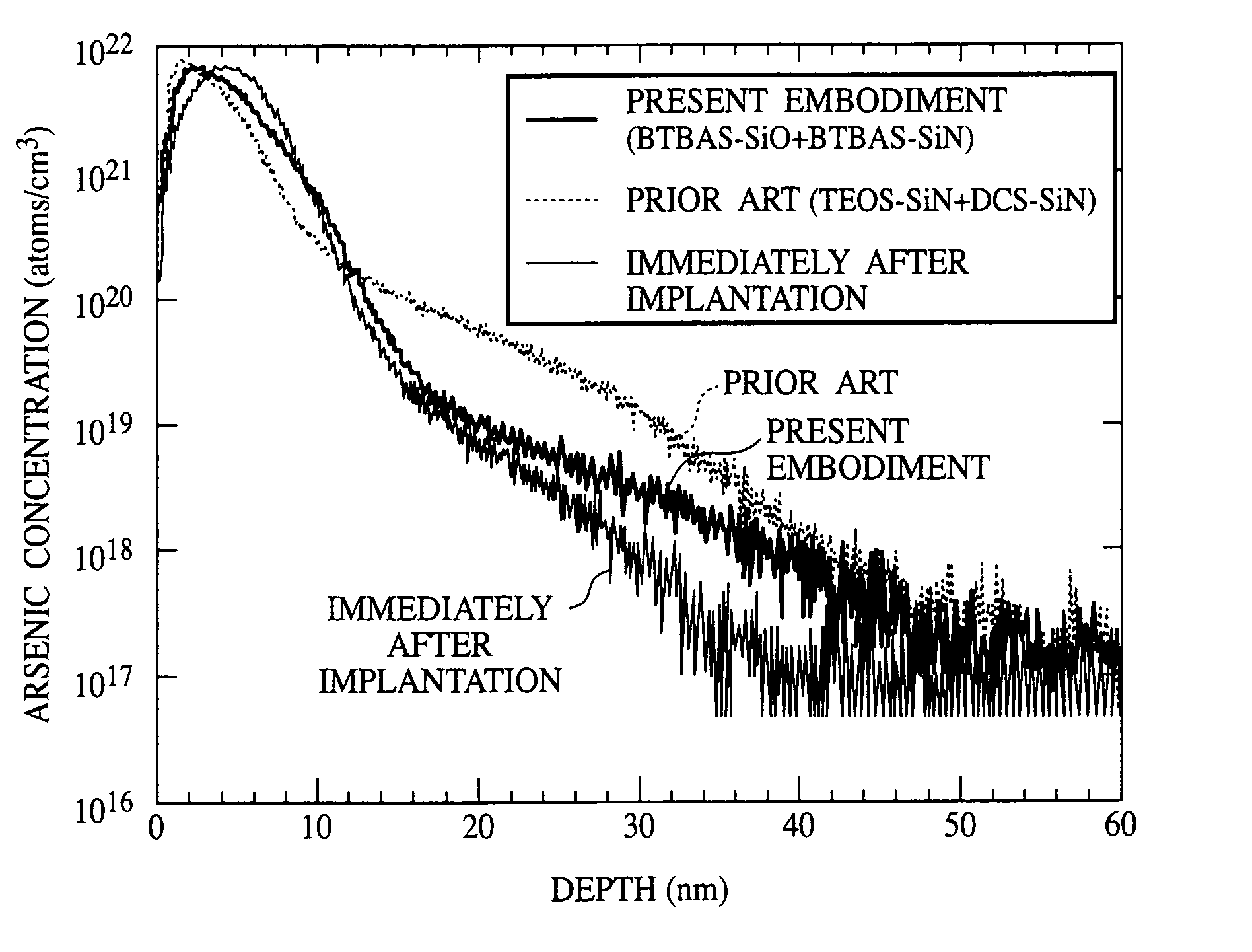
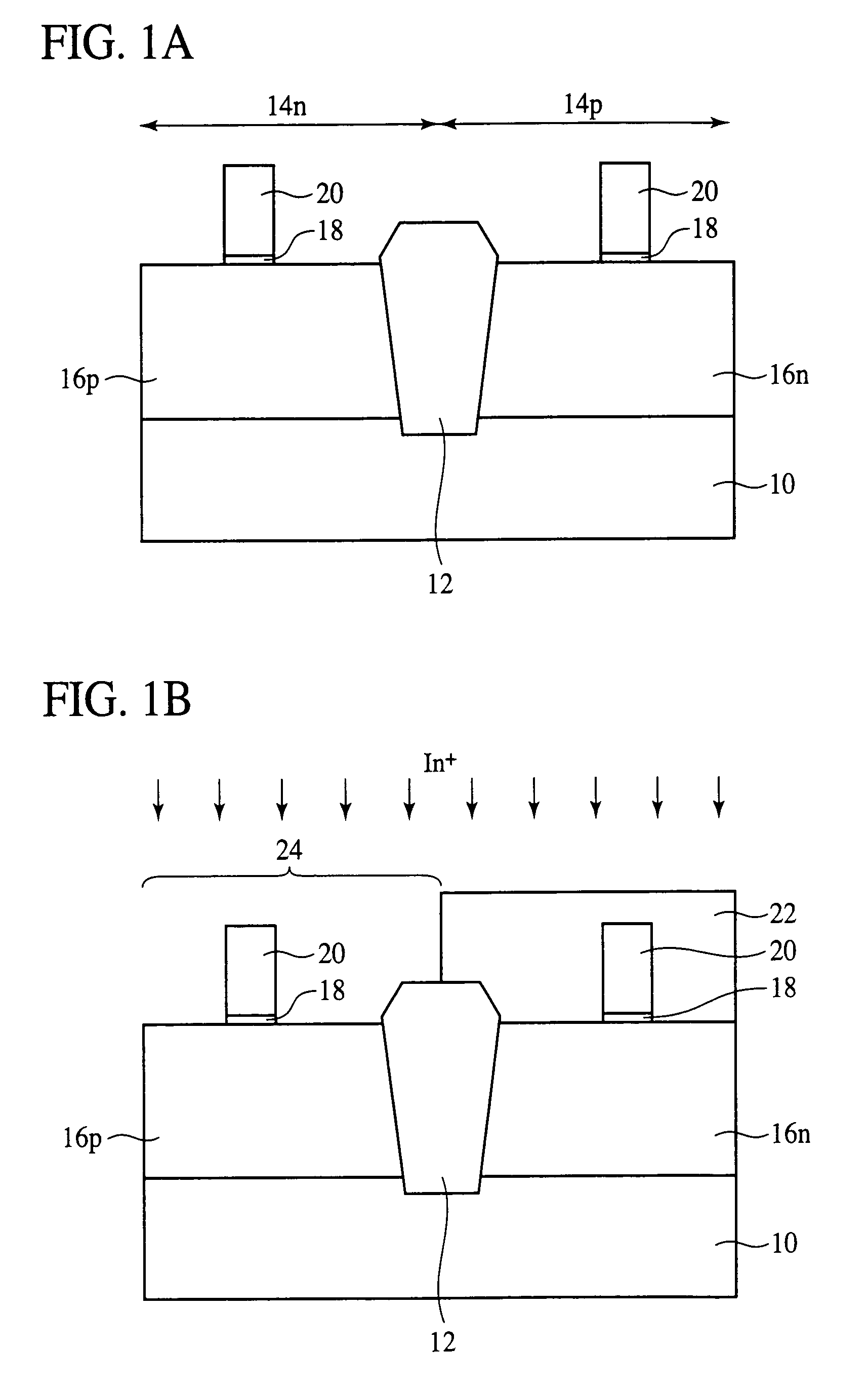
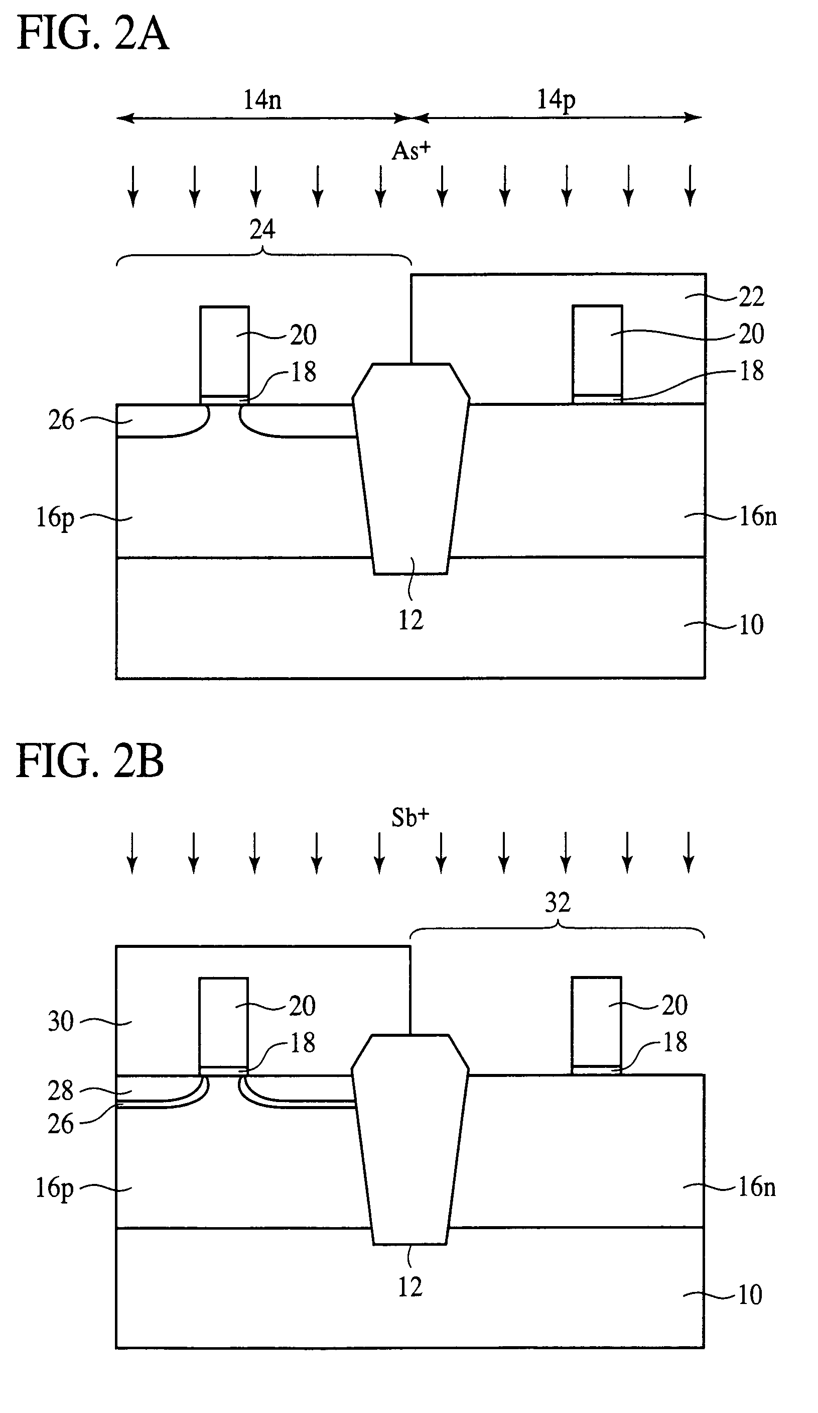
[0073]The semiconductor device fabrication method according to the present invention will be explained with reference to FIGS. 1A to 12. FIGS. 1A to 8 are sectional views of a semiconductor device in the steps of the semiconductor device fabrication method according to the present embodiment, which show the method.
[0074]First, as shown in FIG. 1A, an element isolation region 12 for defining element region is formed on a semiconductor substrate 10, e.g., silicon. The element isolation region 12 can be formed by, e.g., STI (Shallow Trench Isolation).
[0075]Then, a photoresist film (not shown) is formed on the entire surface by, e.g., spin coating.
[0076]Then, an opening (not shown) for opening a region 14n for an NMOS transistor to be formed in is formed in the photoresist film by photolithography.
[0077]Then, with the photo resist film as the mask, a p-type dopant is implanted to thereby a p-type well 16p in the semiconductor substrate 10 in the region 14n, where the NMOS transistor is ...
second embodiment
[0155][A Second Embodiment]
[0156]The semiconductor device fabrication method according to a second embodiment of the present invention will be explained with reference to FIGS. 14A to 21B. FIGS. 14A to 21B are sectional views of a semiconductor device in the steps of the semiconductor device fabrication method according to the present embodiment, which show the method. The same members of the present embodiment as those of the semiconductor device fabrication method are represented by the same reference numbers not to repeat or to simplify their explanation.
[0157]The semiconductor device fabrication method according to the present embodiment is characterized mainly in that dopant diffused regions 48, 56 forming the deep regions of the extension source drain structure are formed before dopant diffused regions 28, 36 forming the shallow regions of the extension source / drain structure are formed.
[0158]The steps of the semiconductor device fabrication method according to the present emb...
third embodiment
[0180][A Third Embodiment]
[0181]Before the semiconductor device fabrication method according to a third embodiment of the present invention is explained, the principle of the semiconductor device fabrication method according to the third embodiment of the present invention will be explained.
[0182]The rate of the film forming reaction for forming a silicon nitride film by CVD using BTBAS and NH3 as raw materials will be determined by 2 steps of feeding N—H to be the N source.
[0183]FIG. 23 is a conceptual view of the film forming mechanism for forming silicon nitride film, using BTBAS and NH3 as raw material gases.
[0184]The first step of feeding the N source is as follows.
[0185]First, as indicated by (1) in FIG. 23, BTBAS molecules are adsorbed on a semiconductor substrate. The BTBAS adsorbed on the semiconductor substrate is decomposed as indicated by (2) in FIG. 23. Specifically, the Si—NHC(CH3)3 bond, whose bond energy is lowest in the molecular structure of BTBAS, is severed to pr...
PUM
| Property | Measurement | Unit |
|---|---|---|
| Temperature | aaaaa | aaaaa |
| Temperature | aaaaa | aaaaa |
| Temperature | aaaaa | aaaaa |
Abstract
Description
Claims
Application Information