Semiconductor device and manufacturing method thereof

a semiconductor and manufacturing method technology, applied in the direction of radiation control devices, identification means, instruments, etc., can solve the problems of low heat resistance of plastic film, easy cracking and heavy above the substrate, and inability to use large-sized glass substrates and large-sized quartz substrates, etc., to achieve high field effect mobility and substantial increase of field effect mobility

Inactive Publication Date: 2007-02-20
SEMICON ENERGY LAB CO LTD
View PDF46 Cites 319 Cited by
  • Summary
  • Abstract
  • Description
  • Claims
  • Application Information

AI Technical Summary

Benefits of technology

[0011]According to the present invention, when a layer to be peeled including elements is formed on a substrate, all channel length directions of regions which serve as channels of the elements are aligned with the same direction and laser light irradiation is conducted for scanning in the same direction as the channel length direction to complete the elements. After that, the layer to be peeled is bonded to a base member having a curved surface which is bent in a direction different from the channel length direction, that is, in a channel width direction to realize a display having a curved surface. Note that, when the layer to be peeled is bonded to the base member having the curved surface, it is bent along the curved surface of the base member. According to the present invention, all channel length directions of the elements are aligned with the same direction and the channel length directions are different from a direction in which the base member is bent. Thus, even if the layer to be peeled including the elements is bent, the influence on element characteristics can be minimized. In other words, a semiconductor device which is resistant to deformation in a predetermined direction (here, the direction in which the base member is bent) can be provided.
[0023]Also, as another peeling method, a peeling method of conducting peeling by utilizing film stresses of two layers may be used. According to this peeling method, a metallic layer, preferably, a metallic nitride layer is provided on a substrate, an oxide layer is provided in contact with the metallic nitride layer, and an element is produced on the oxide layer. Thus, even when film formation processing or heat treatment at 500° C. or higher is performed, film peeling is not caused. As a result, clean separation can be easily produced in an inner portion of the oxide layer or interface thereof by a physical means. In order to further promote peeling, heat treatment or laser light irradiation processing may be performed before the peeling is conducted by the physical means.
[0029]Also, in the above respective constitutions, the channel length directions are the same direction as a scanning direction of laser light irradiated to a semiconductor layer composing the thin film transistors. In the case where a channel of the thin film transistor which is made from a semiconductor film crystallized by laser annealing is formed on a substrate, when a crystal growth direction is aligned with a carrier moving direction, high field effect mobility can be obtained. In other words, when the crystal growth direction is aligned with the channel length direction, the field effect mobility can be substantially increased. When a continuous oscillating laser beam is irradiated to a non-single crystalline semiconductor film for crystallization, a solid-liquid interface is kept. Thus, a continuous crystal growth can be produced in the scanning direction of the laser beam. For the laser light, a gas laser such as an excimer laser, a solid laser such as a YAG laser, or a semiconductor laser is preferably used. In addition, a laser oscillation mode may be either continuous oscillation or pulse oscillation. A laser beam may have a linear shape or a rectangular shape.

Problems solved by technology

However, there is a defect that the above substrate is easy to crack and heavy.
In addition, in the case of mass production, it is difficult and thus not suitable to use a large size glass substrate and a large size quartz substrate.
However, the plastic film has a low heat resistance, so that it is necessary to reduce a maximum temperature of a process.
Therefore, a liquid crystal display device and a light emitting element for which the plastic film is used and which each have a high performance are not realized.

Method used


Image

  • Semiconductor device and manufacturing method thereof
  • Semiconductor device and manufacturing method thereof
  • Semiconductor device and manufacturing method thereof

Examples


embodiment 1

[Embodiment 1]

[0064]Here, an example of laser processing apparatus suitable to the present invention will be described.

[0065]Crystallization of amorphous silicon by laser annealing is conducted through a melting-solidification process. More specifically, the case where it is divided into two stages, that is, a stage of generation of crystal nucleus and a stage of crystal growth from the nucleus is considered. However, in the case of laser annealing using a pulse laser beam, a generation position of crystal nucleus and a generation density thereof cannot be controlled but left to natural generation. Thus, a crystal grain is formed at an arbitrary position within the surface of a glass substrate and only a small size of about 0.2 μm to 0.5 μm is obtained. A large number of defects are caused in a crystal boundary. This is considered to be a factor limiting the field effect mobility of a TFT.

[0066]It is considered that a method of conducting crystallization with melting solidification ...

embodiment 2

[Embodiment 2]

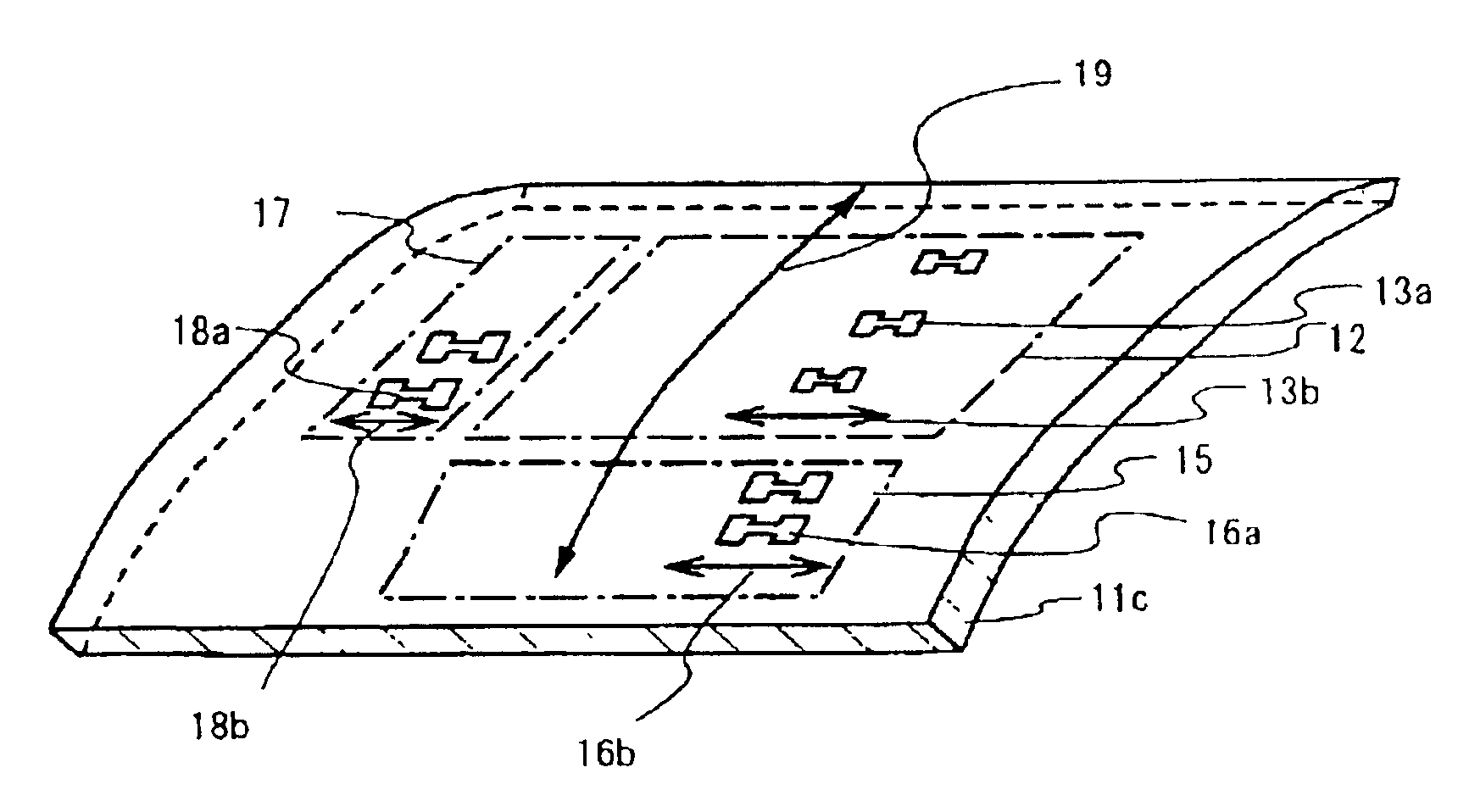
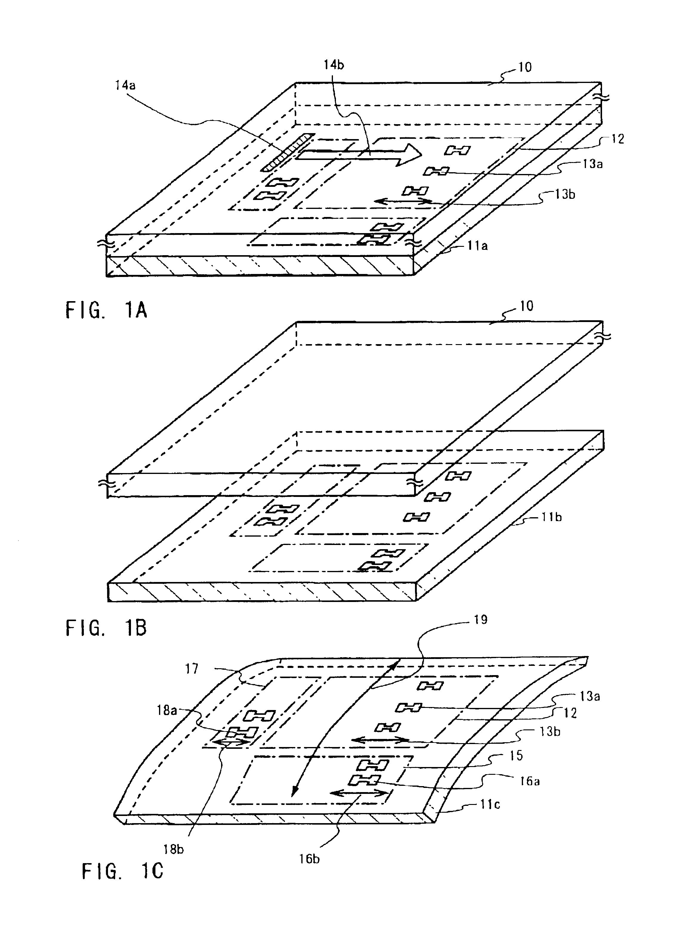
[0096]The example of the top gate TFT is descried in Embodiment 1. Here, an example of a bottom gate TFT will be described. Also, the structure except for the TFT is the same one as Embodiment 1 and the description is thereof omitted here.

[0097]Next, steps of crystallizing a non-single crystalline semiconductor film and producing a TFT from the formed crystalline semiconductor film will be descried with reference to FIGS. 7A to 7D.

[0098]FIG. 7B is a longitudinal cross sectional view. A non-single crystalline semiconductor film 503 is formed on a gate insulating film 506 covering a gate electrode. A typical example of the non-single crystalline semiconductor film 503 is an amorphous silicon film. In addition, an amorphous silicon germanium film or the like can be applied. The thickness of 10 nm to 200 nm can be applied and may be further increased in accordance with a wavelength of a laser beam and an energy density thereof. In addition, it is desirable to employ such a...

embodiment 3

[Embodiment 3]

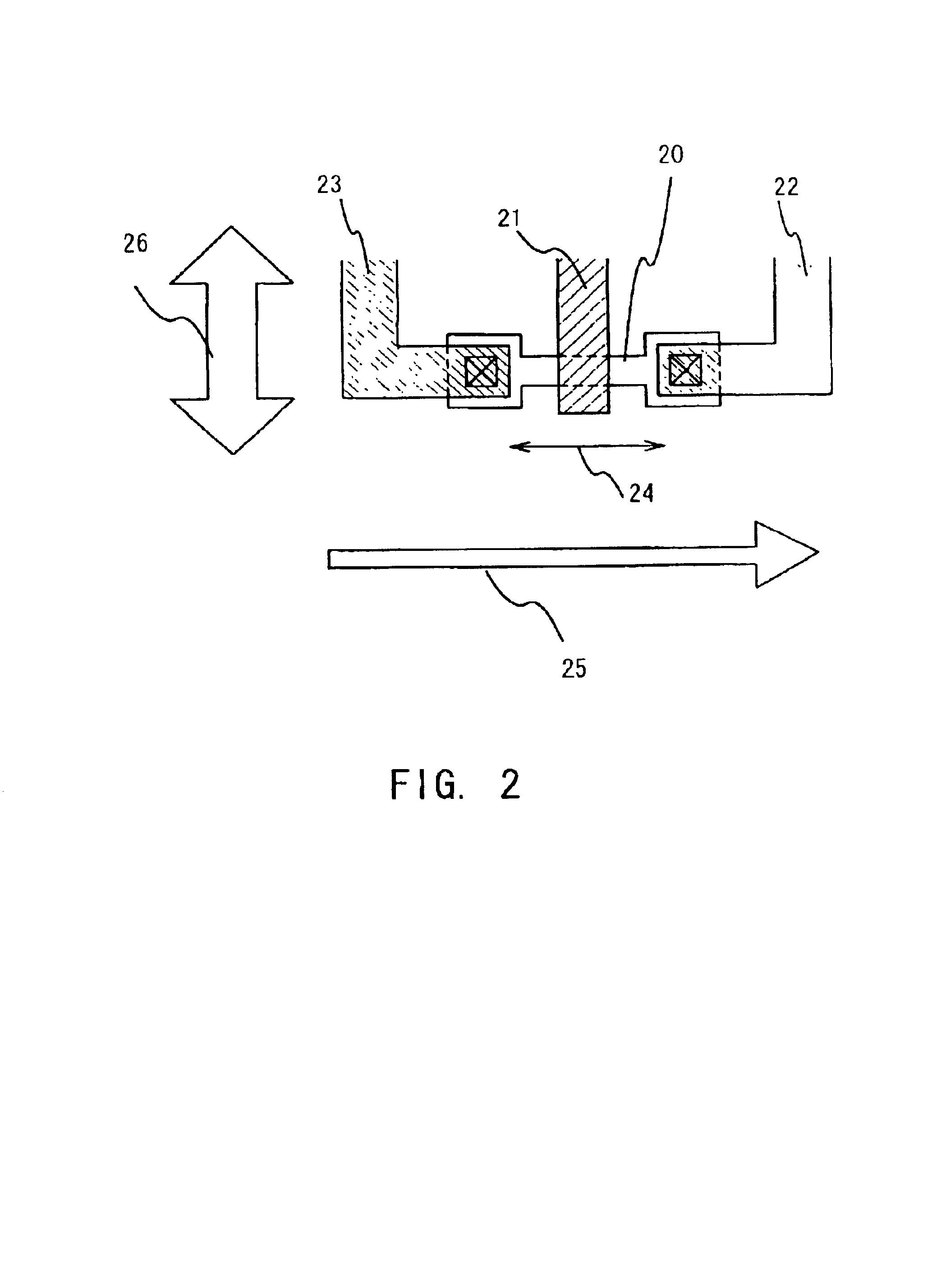
[0110]The peeling method of conducting peeling by utilizing film stresses of two layers (stress strain) is used in Embodiments 1 and 2. A peeling method is not particularly limited. For example, a method of providing a separate layer between the layer to be peeled and the substrate and removing the separate layer by a chemical solution (etchant) to separate the layer to be peeled and the substrate can be used. Alternatively, there can be used a method of providing a separate layer made of amorphous silicon (or polysilicon) between the layer to be peeled and the substrate and irradiating laser light thereto through the substrate to release hydrogen contained in the amorphous silicon, thereby producing gaps to separate the layer to be peeled and the substrate.

[0111]Here, an example in which amorphous silicon (or polysilicon) containing a large amount of hydrogen is used for the separate layer and laser light is irradiated to the separate layer for peeling is shown in FIG...


PUM

PropertyMeasurementUnit
thicknessaaaaaaaaaa
temperatureaaaaaaaaaa
thicknessesaaaaaaaaaa

Abstract

The invention relates to a semiconductor device including a plurality of thin film transistors provided on a base member having a curved surface. The surface may be bent in either a convex shape or a concave shape. All channel length directions of the plurality of thin film transistors may also be aligned in the same direction. Further, the channel length direction may be different from the direction in which the base member is bent. A pixel portion and a driver circuit portion may also be provided on the base member. The invention also includes a method of manufacturing a semiconductor device including forming a layer to be peeled including an element of a substrate, bonding a support member to the layer to be peeled, and bonding a transfer body to the layer to be peeled.

Description

BACKGROUND OF THE INVENTION[0001]1. Field of the Invention[0002]The present invention relates to a semiconductor device having a circuit composed of thin film transistors (hereinafter referred to as TFTs) transferred by bonding a peeled layer (to be peeled) to a base member and a manufacturing method thereof. More particularly, the present invention relates to an electro-optical device which is represented by a liquid crystal module, a light emitting device which is represented by an EL module, and electronic equipment on which such a device is mounted as a part.[0003]Note that a semiconductor device in this specification indicates general devices functioning by utilizing semiconductor characteristics, and an electro-optical device, a light emitting device, a semiconductor circuit, and electronic equipment are all semiconductor devices.[0004]2. Description of the Related Art[0005]In recent years, a technique of constructing a thin film transistor (TFT) using a semiconductor thin fil...

Claims


Application Information

Patent Timeline
Patent Type & Authority Patents(United States)
IPC IPC(8): H01L29/04H01L31/036H01L31/0376H01L31/20G02F1/1333G02F1/1362G02F1/1368G09F9/00G09F9/30G09F9/35H01L21/02H01L21/20H01L21/268H01L21/336H01L21/77H01L21/84H01L27/08H01L27/12H01L27/32H01L29/786
CPCH01L27/1214H01L29/78603H01L29/78696H01L27/1266G02F1/133305G02F1/13454G02F2001/13613H01L2924/3511H01L27/3244H01L27/1285H01L27/1218G02F1/13613H10K59/12
Inventor YAMAZAKI, SHUNPEITAKAYAMA, TORU
Owner SEMICON ENERGY LAB CO LTD
Why Eureka
Try Eureka