Method of manufacturing potassium niobate single crystal thin film, surface acoustic wave element, frequency filter, frequency oscillator, electronic circuit, and electronic apparatus

a single crystal, potassium niobate technology, applied in the direction of crystal growth process, polycrystalline material growth, chemically reactive gases, etc., can solve the problems of low ksup>2/sup>, low ksup>2/sup>, and inability to achieve excellent surface morphology, so as to reduce size and save power , the effect of reducing the siz

Inactive Publication Date: 2007-08-21
SEIKO EPSON CORP
View PDF8 Cites 5 Cited by
  • Summary
  • Abstract
  • Description
  • Claims
  • Application Information

AI Technical Summary

Benefits of technology

[0018]Preferably, the substrate includes an axis on a surface thereof that is oriented in a vertical direction and in an in-plane direction to the surface, and the single crystal is grown epitaxially on the substrate. According to the method, the potassium niobate single crystal thin film can be obtained that has a uniform orientation over the entire thin film with the substrate as a seed crystal. Therefore, using the potassium niobate single crystal thin film, a surface acoustic wave element having an excellent k2 can be manufactured.
[0019]Advantageously, the substrate has a larger coefficient of thermal expansion than that of potassium niobate, and has a perovskite-type pseudo-cubic unit cell that is oriented in an in-plane (100) direction on an entire surface of the substrate. Moreover, the substrate is a strontium titanate (100) single crystal substrate. According to the method, the potassium niobate single crystal is precipitated in orthorhombic (110) orientation on the substrate. In addition, using the strontium titanate (100) single crystal substrate, which is a perovskite-type oxide single crystal substrate in a wide use, a potassium niobate single crystal thin film having good surface morphology can be obtained. An excellent surface acoustic wave element having a maximum value of about 30% for k2 can be manufactured.
[0022]Preferably, the substrate includes a body that is composed of one of quartz, crystal, SiO2-covered silicon, and diamond-covered silicon, and a buffer layer formed thereon, and wherein the buffer layer contains a first buffer layer grown in in-plane orientation independently of crystal orientation of the substrate and a second buffer layer of an oxide grown epitaxially on the first buffer layer, the first and second buffer layers being manufactured by a vapor deposition method accompanying ion beam radiation. According to the method, the high-quality potassium niobate single crystal thin film can be manufactured even on a substrate made of a material such as quartz, crystal, SiO2-covered silicon, or diamond-covered silicon that is inexpensive and appropriate for a surface acoustic wave element. By the use of the potassium niobate single crystal thin film, an excellent surface acoustic wave element having a maximum value of 50% for k2 can be manufactured.
[0023]Preferably, the first buffer layer is composed of a NaCl-type oxide, and the second buffer layer is composed of a simple perovskite-type oxide. In addition, the first buffer layer is composed of a fluorite-type oxide, and the second buffer layer is composed of a laminated perovskite-type oxide and a simple perovskite-type oxide grown epitaxially on the laminated perovskite-type oxide. According to the method, the high-quality potassium niobate single crystal thin film can be manufactured on a substrate made of an inexpensive material such as quartz, crystal, SiO2-covered silicon, or and diamond-covered silicon. Making use of the potassium niobate single crystal thin film, an excellent surface acoustic wave element having a value closer to a theoretical maximum value of about 50% for k2 can be manufactured.
[0024]A surface acoustic wave element in accordance with the invention includes a potassium niobate single crystal thin film produced by the manufacturing method of the invention previously mentioned. The potassium niobate single crystal thin film having a large k2 enables reduction in size of the surface acoustic wave element.
[0026]An electronic circuit in accordance with the invention includes a frequency oscillator of the invention previously mentioned. The frequency oscillator has a filter of wide band characteristics, is reduced in size, and saves power. An electronic apparatus in accordance with the invention includes at least one of a frequency filter, a frequency oscillator, and an electronic circuit of the invention previously mentioned. The electronic apparatus provides a reduction in size power-saving, and wideband system.

Problems solved by technology

Thus, when only a KNbO3 single crystal substrate is used, the sound velocity, high k2, and zero temperature properties cannot all be satisfied.
However, the simple application of the tri-phase-epitaxy method to the manufacturing of a KNbO3 single crystal thin film did not allow selective etching of the residue of the liquid phase 3K2O.Nb2O5 after a single crystal thin film was grown.
Accordingly, since the liquid phase remained on the surface of the single crystal, a thin film having an excellent surface morphology could not be obtained.

Method used


Image

  • Method of manufacturing potassium niobate single crystal thin film, surface acoustic wave element, frequency filter, frequency oscillator, electronic circuit, and electronic apparatus
  • Method of manufacturing potassium niobate single crystal thin film, surface acoustic wave element, frequency filter, frequency oscillator, electronic circuit, and electronic apparatus
  • Method of manufacturing potassium niobate single crystal thin film, surface acoustic wave element, frequency filter, frequency oscillator, electronic circuit, and electronic apparatus

Examples


first embodiment

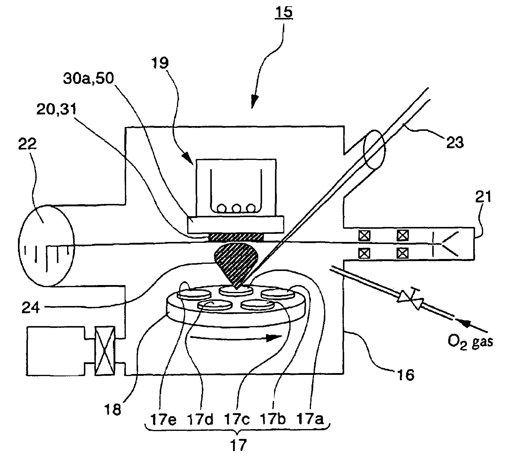
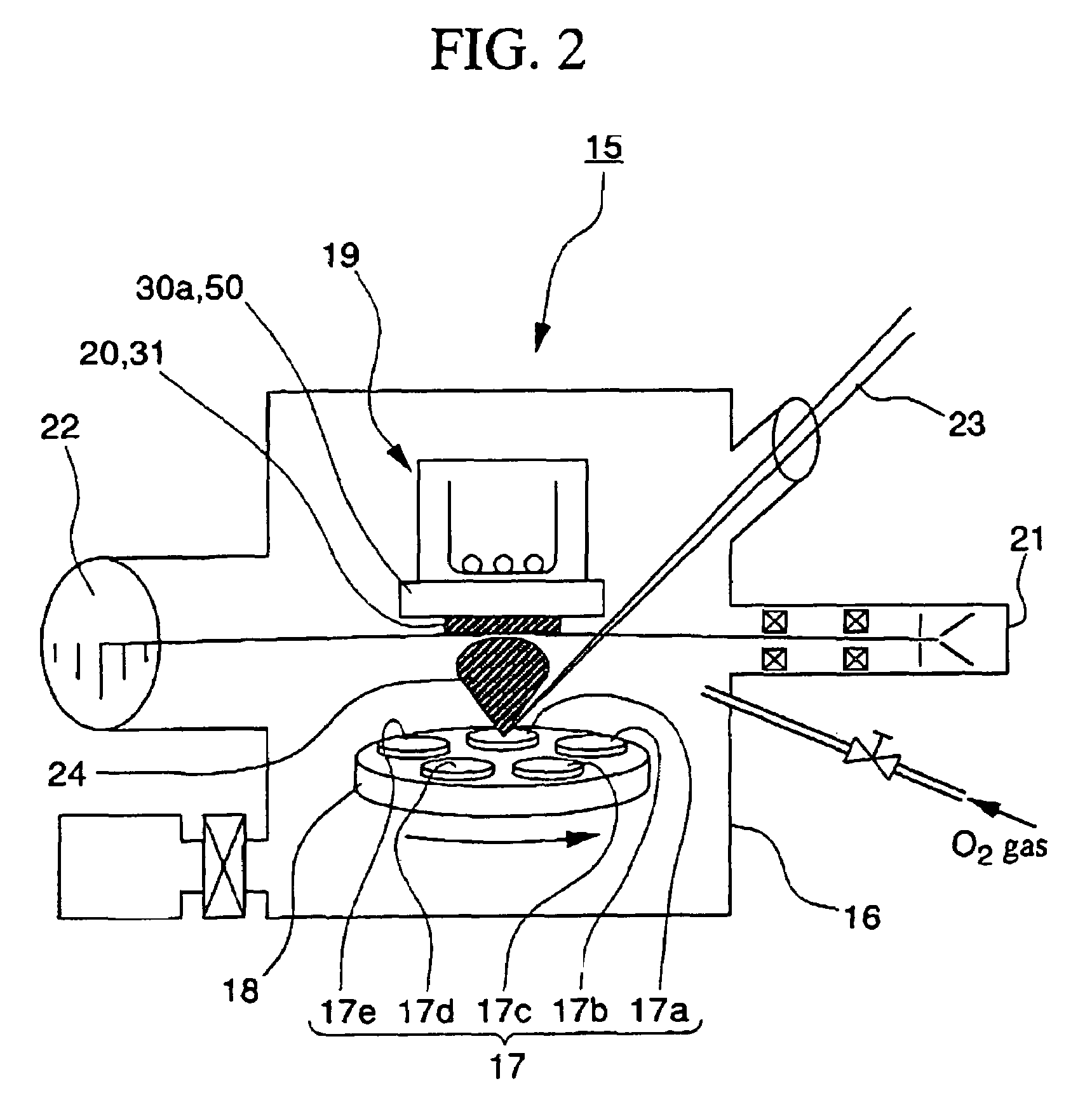
[0048]FIG. 2 is a perspective view of a deposition apparatus 15 for the The KNbO3 single crystal layer 12 is manufactured by a vapor deposition using ion beam radiation. A thin film in the embodiment is formed by a pulsed laser deposition (PLD) method. An apparatus 15 used for forming the film, as shown in FIG. 2, includes a process chamber 16 in which pressure can be reduced, at least one workpiece 17 placed opposite to the SrTiO3 single crystal substrate 13, a workpiece support unit 18 that supports and rotates the workpiece 17 thereon and enables the workpiece 17 to revolve on its own axis, and a holding unit 19 for holding the SrTiO3 single crystal substrate 13. The deposition apparatus 15 contains a reflection high energy electron diffraction (RHEED) source 21 used for analyzing a thin film 20 in a RHEED method, and an RHEED screen 22 for detecting beams reflected by the thin film 20 that are emitted by the RHEED source 21 to the thin film 20 deposited on the SrTiO3 single cry...

second embodiment

[0064]The silicon single crystal substrate 31a has a coefficient of thermal expansion of 3.0×10⁻⁶ (K−1), which is larger than a coefficient of thermal expansion of 0.5×10⁻⁶ (K−1) for a b-axis of the KNbO3 single crystal layer 12, but is smaller than coefficients of thermal expansion 5.0×10⁻⁶ (K−1) for an a-axis and 14.1×10⁻⁶ (K−1) for a c-axis. The substrate surface is coated by a naturally oxidized film. FIG. 7 is a cross-sectional view of KNbO3 thin film in the The buffer layer 32, as shown in FIG. 7, includes a first buffer layer 34 and a second buffer layer 35 epitaxially grown on the first buffer layer 34. The first buffer layer 34 contains a first buffer layer 34a having yttria-stabilized zirconia (YSZ) and a first buffer layer 34b having CeO2 epitaxially grown on the first buffer layer 34a.

[0065]The first buffer layer 34a and the first buffer layer 34b are composed of a metallic oxide, which may be a NaCl structure or fluorite structure. In particular, the following is pref...


PUM

PropertyMeasurementUnit
melting pointaaaaaaaaaa
eutectic temperatureaaaaaaaaaa
pressureaaaaaaaaaa

Abstract

A method of manufacturing KNbO3 single crystal thin film having single-phase high quality and excellent morphology on each of single crystal substrates. A surface acoustic wave element, frequency filter, frequency oscillator, electronics circuit, and electronic device employ the thin film manufactured by the method, and have high k2, and are wideband, reduced in size and economical in power consumption. A plasma plume containing K, Nb, and O in the range 0.5≦x≦xE is supplied to a substrate, where x is a mole ratio of niobium (Nb) to potassium (K) in KxNb1−xOy, and xE is a mole composition ratio at the eutectic point for KNbO3 and 3K2O.Nb2O5 under a predetermined oxygen partial pressure. Maintaining the temperature Ts of the substrate in the range TE≦Ts≦Tm where TE represents the temperature at the eutectic point and Tm represents a complete melting temperature, the KNbO3 single crystal is precipitated from the KxNb1−xOy deposited on the substrate.

Description

PRIORITY CLAIM[0001]This application is a continuation-in-part application based on U.S. patent application Ser. No. 10 / 808,250 filed on Mar. 24, 2004, and priority is claimed on Japanese Patent Application No. 2003-085761 filed on Mar. 26, 2003, the contents of which are incorporated herein by reference.BACKGROUND OF THE INVENTION[0002]1. Field of the Invention[0003]The present invention relates to a method of manufacturing potassium niobate single crystal thin films, and to surface acoustic wave elements, frequency filters, frequency oscillators, electronic circuits, and electronic apparatuses, each having the potassium niobate single crystal thin film.[0004]2. Description of Related Art[0005]There has been a remarkable expansion in the demand for surface acoustic wave elements with rapid developments in telecommunications centered on mobile communication, which is typified by mobile telephones. Some trends in the development of surface acoustic wave elements include size reductio...

Claims


Application Information

Patent Timeline
Patent Type & Authority Patents(United States)
IPC IPC(8): C30B25/02C30B19/00C30B19/12H03H3/08H03H9/02H03H9/05
CPCC30B19/00C30B19/12H03H3/08H03H9/02543H03H9/02574H03H9/0542C30B29/30
Inventor HIGUCHI, TAKAMITSUIWASHITA, SETSUYAMIYAZAWA, HIROMU
Owner SEIKO EPSON CORP
Why Eureka
Try Eureka