Silicon annealed wafer and silicon epitaxial wafer

a technology of silicon epitaxial wafers and annealing wafers, which is applied in the direction of after-treatment details, silicon compounds, transportation and packaging, etc., can solve the problems of deterioration of device characteristics, increase of production costs, and inability to remove such cop defects from the wafers, so as to reduce the size of cop defects, reduce the effect of pass time and suppress the occurrence of large cop defects

Active Publication Date: 2007-09-25
SUMITOMO MITSUBISHI SILICON CORP
View PDF7 Cites 13 Cited by
  • Summary
  • Abstract
  • Description
  • Claims
  • Application Information

AI Technical Summary

Benefits of technology

[0025]The expansion of the annular potential region of OSF occurrence toward the center of the wafer causes the density of BMDs to be altered in the distribution on the surface of the wafer, so that the difference between the maximum and minimum of the BMD density is increased and therefore the uneven distribution becomes nonuniformer. A further increased amount of doped nitrogen causes the OSF density to be increased, thereby distribution becoming uniform over the entire surface area of the wafer.
[0048]As described above, using a pulling apparatus providing an improved temperature distribution at a high temperature just after pulling the single crystal in the growth of a single crystal, a small amount of doped nitrogen and a further shortened pass time within the low temperature range make it possible to obtain a wafer including small size COP defects and uniformly distributed BMDs.

Problems solved by technology

The existence of such BMDs in the surface region of the wafer, on which devices are formed, i.e., on an active region, causes the deterioration of the device characteristics.
However, long process times for the heat treatment and a large variation in the effect of the treatment result in an increase of the production cost.
In most cases, moreover, COP (Crystal Originated Particle) defects (which are called IR-light scattering tomography defects when they exist in the wafer), which pertain to a type of grown-in defects formed in the course of growing a single crystal, reside in the wafer, and it is not possible to remove such COP defects from the wafer by the DZ-IG treatment.
A main factor of deteriorating the device characteristics results from the COP defects in the current process of manufacturing semiconductor devices.
However, due to the high segregation coefficient of nitrogen, it is difficult to distribute nitrogen concentration uniformly over the entire single crystal to be grown.
Consequently, if it is necessary to dope nitrogen in the single crystal at a high concentration, the crystal area at such high concentration is restricted and no satisfactory yield can be obtained, thereby making it difficult to apply this method to the practical usage.

Method used


Image

  • Silicon annealed wafer and silicon epitaxial wafer
  • Silicon annealed wafer and silicon epitaxial wafer
  • Silicon annealed wafer and silicon epitaxial wafer

Examples


examples

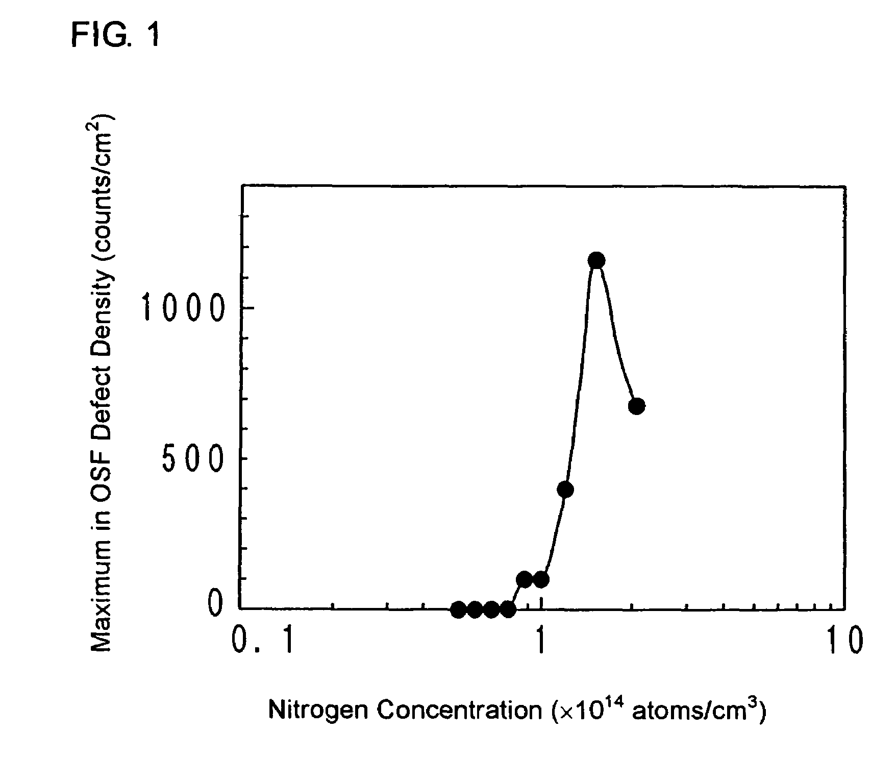
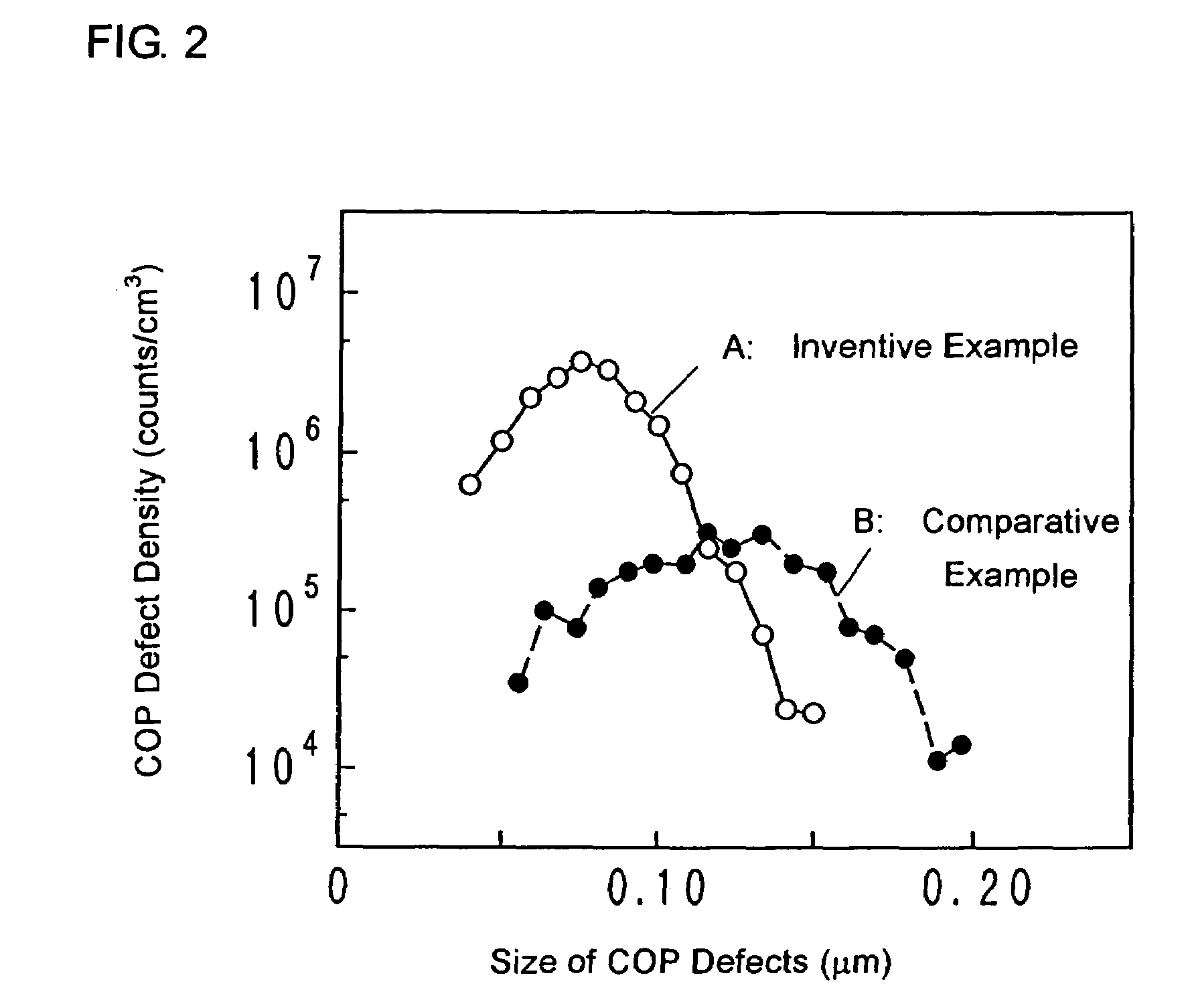
[0093]Utilizing a Czochralski furnace capable of varying the cooling conditions in the hot zone, a p-type silicon single crystal having a diameter of 200 mm, a resistivity of 10 Ωcm and an oxygen concentration of approximately 14×1017 atoms / cm3 was grown, varying the following parameters in the growth conditions: the nitrogen doping concentration; the temperature gradient ratio Gc / Ge at a temperature range from 1370° C.-1310° C.; the pass time from 1200° C. to 1000° C.; and the pass time from 1030° C. to 920° C. The conditions for growing a single crystal in trial are listed in Table 1.

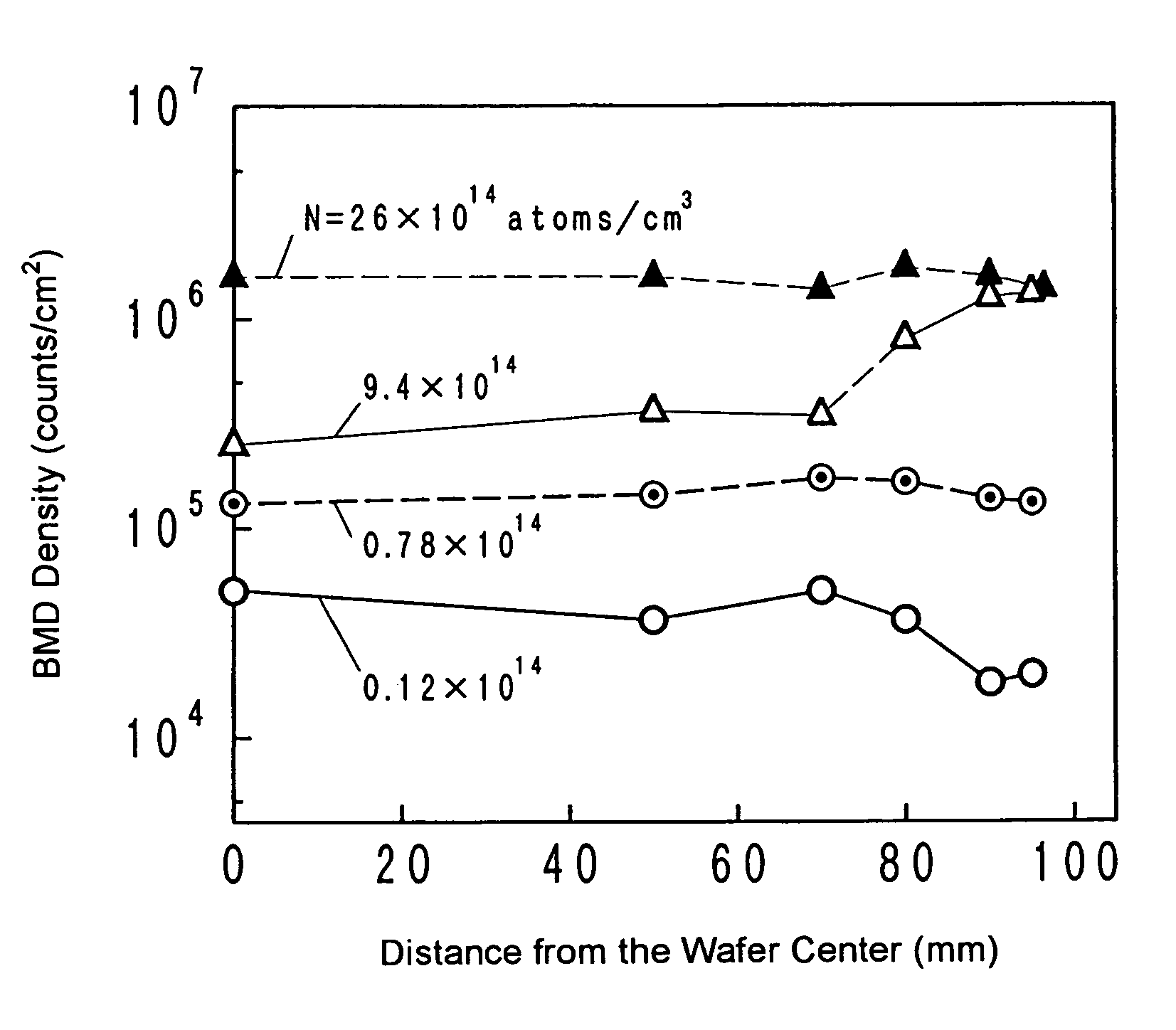
[0094]Each grown single crystal was sliced into disk-shaped test pieces. These test pieces were subjected to a heat treatment at 650° C. for 30 min in a nitrogen gas atmosphere, and then wafers were produced from the test pieces. The following characteristics were determined by measurements for each of the test specimens: The size and distribution of COP defects; the BMD density distribution; and the ...


PUM

PropertyMeasurementUnit
thicknessaaaaaaaaaa
sizeaaaaaaaaaa
sizeaaaaaaaaaa

Abstract

A silicon annealed wafer having a sufficient thick layer free from COP defects on the surface, and a sufficient uniform BMD density in the inside can be produced by annealing either a base material wafer having nitrogen at a concentration of less than 1×10¹⁴ atoms / cm3, COP defects having a size of 0.1 μm or less in the highest frequency of occurrence and no COP defects having a size of 0.2 μm or more, oxygen precipitates at a density of 1×10⁴ counts / cm2 or more, and BMDs (oxygen precipitates), where the ratio of the maximum to the minimum of the BMD density in the radial direction of the wafer is 3 or less, or a base material wafer grown at specific average temperature gradients within specific temperature ranges and specific cooling times for a single crystal at a nitrogen concentration of less than 1×10¹⁴ atoms / cm3, employing the Czochralski method. Moreover, a silicon epitaxial wafer having very small defects and a uniform BMD distribution in the inside can be formed by growing an epitaxial layer on the surface of either the first type base material wafer or the second type base material wafer. Both the silicon annealed wafer and the silicon epitaxial wafer greatly reduce the rate of producing defective devices, thereby enabling the device productivity to be enhanced.

Description

BACKGROUND OF THE INVENTION[0001]1. Field of the Invention[0002]The present invention relates to a silicon annealed wafer having a defect free layer on the surface, which wafer is used for producing semiconductor devices, and also to a silicon epitaxial wafer with a perfect epitaxial layer.[0003]2. Description of the Related Art[0004]A silicon wafer used for producing semiconductor devices is produced by slicing a silicon single crystal grown mainly by the Czochralski method. In the Czochralski method, a silicon single crystal is grown from molten silicon in a quartz crucible, pulling up a seed crystal to solidify the molten silicon.[0005]Normally, oxygen solves into the molten silicon from the raw silicon material and / or the quartz crucible, and the solved oxygen is retained in the single crystal during the silicon solidification. The solubility of oxygen is decreased by the decrease in the temperature of the single crystal, and therefore the single crystal contains oxygen in a sat...

Claims


Application Information

Patent Timeline
Patent Type & Authority Patents(United States)
IPC IPC(8): B32B9/04C30B29/06C30B33/00H01L21/20H01L21/322
CPCC30B29/06H01L21/3225C30B33/00Y10T428/21
Inventor NISHIKAWA, HIDESHITAKASE, NOBUMITSUEGASHIRA, KAZUYUKIHAYAKAWA, HIROSHI
Owner SUMITOMO MITSUBISHI SILICON CORP
Why Eureka
Try Eureka