Elastomeric mask and use in fabrication of devices

a technology of elastomeric masks and devices, applied in the field of surface modification, can solve the problems of requiring relatively sophisticated and expensive apparatus, requiring excessive number of steps or potentially destructive chemical techniques, and requiring relatively complex apparatus, etc., and achieves the effect of not being well-suited to creating multi-colored displays

Inactive Publication Date: 2007-10-16
PRESIDENT & FELLOWS OF HARVARD COLLEGE +1
View PDF57 Cites 88 Cited by
  • Summary
  • Abstract
  • Description
  • Claims
  • Application Information

AI Technical Summary

Benefits of technology

[0029]Another method of the invention involves immobilizing on average less than about 1×10⁵ at each of a plurality of separate, isolated regions of a surface of an article while leaving regions of the surface of the article intervening the separate isolated regions essentially free of the molecules.
[0030]In another aspect the invention provides an article that can be used for methods described herein or for other purposes. In one embodiment the article is an elastomeric article including a first surface and an opposing second surface, and plurality of channels passing through the article and connecting the first surface with the second surface. At least one of the plurality of channels has a cross-sectional dimension of less than one millimeter.

Problems solved by technology

While the above-described and other techniques may be advantageous in many circumstances, many require relatively sophisticated and expensive apparatus and / or require excessive numbers of steps or potentially destructive chemical techniques.
For example, laser ablation is relatively slow and requires relatively complex apparatus.
Also, it is limited in that pixels are defined by patterning cathode material rather than the electroluminescent material itself, and therefore the technique is not well-suited to creation of a multi-colored display.
However, wet chemical etching generally is required to define pixels using photolithography, which has a deleterious effect on electroluminescent efficiency.
Encapsulation, however, is problematic, according to Tian, et al., who report that it can lead to shorting of devices.
Shadow masking techniques that are known typically involve the use of machined-metal masks, in which the size of pixels are generally considered too large for high-resolution displays.
In many of the above techniques, it is not possible to fabricate displays on non-planar surfaces.
Described above are several techniques for creation of a variety of materials, including electroluminescent materials, that in many cases are complicated and expensive.
Also described above are several masking techniques, many of which do not recognize application to very small-feature, very high-resolution techniques.

Method used


Image

  • Elastomeric mask and use in fabrication of devices
  • Elastomeric mask and use in fabrication of devices
  • Elastomeric mask and use in fabrication of devices

Examples


example 1

Fabrication of a Mask

[0089]A polydimethylsiloxane (PDMS) mask was fabricated.

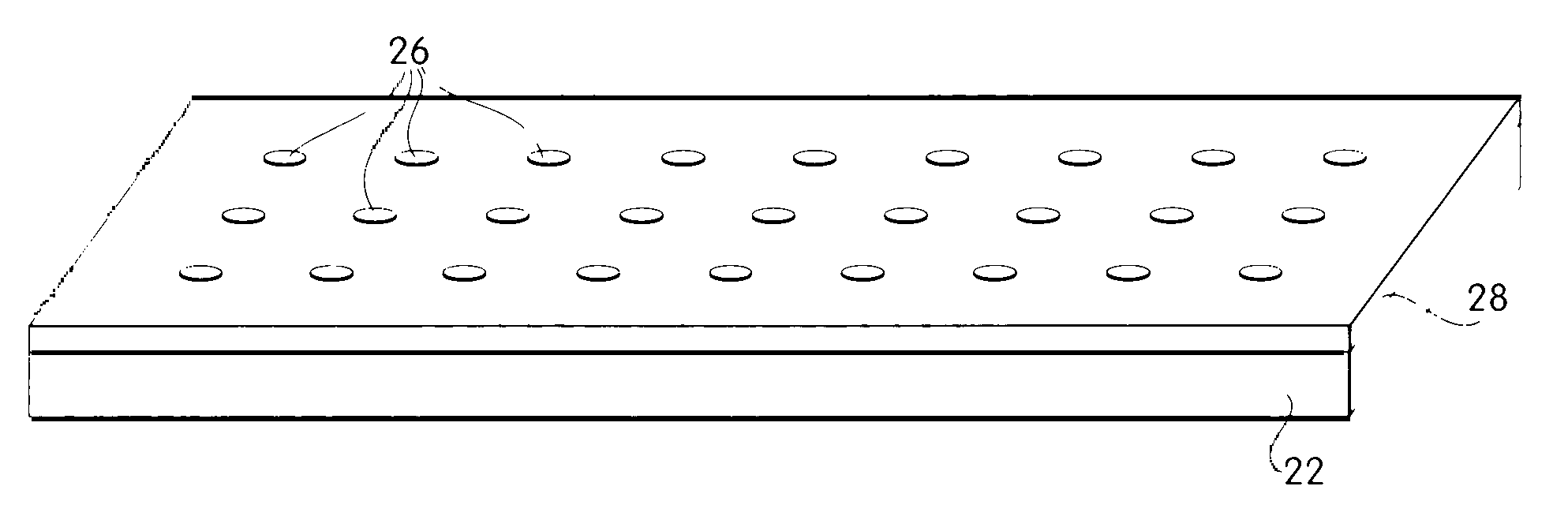
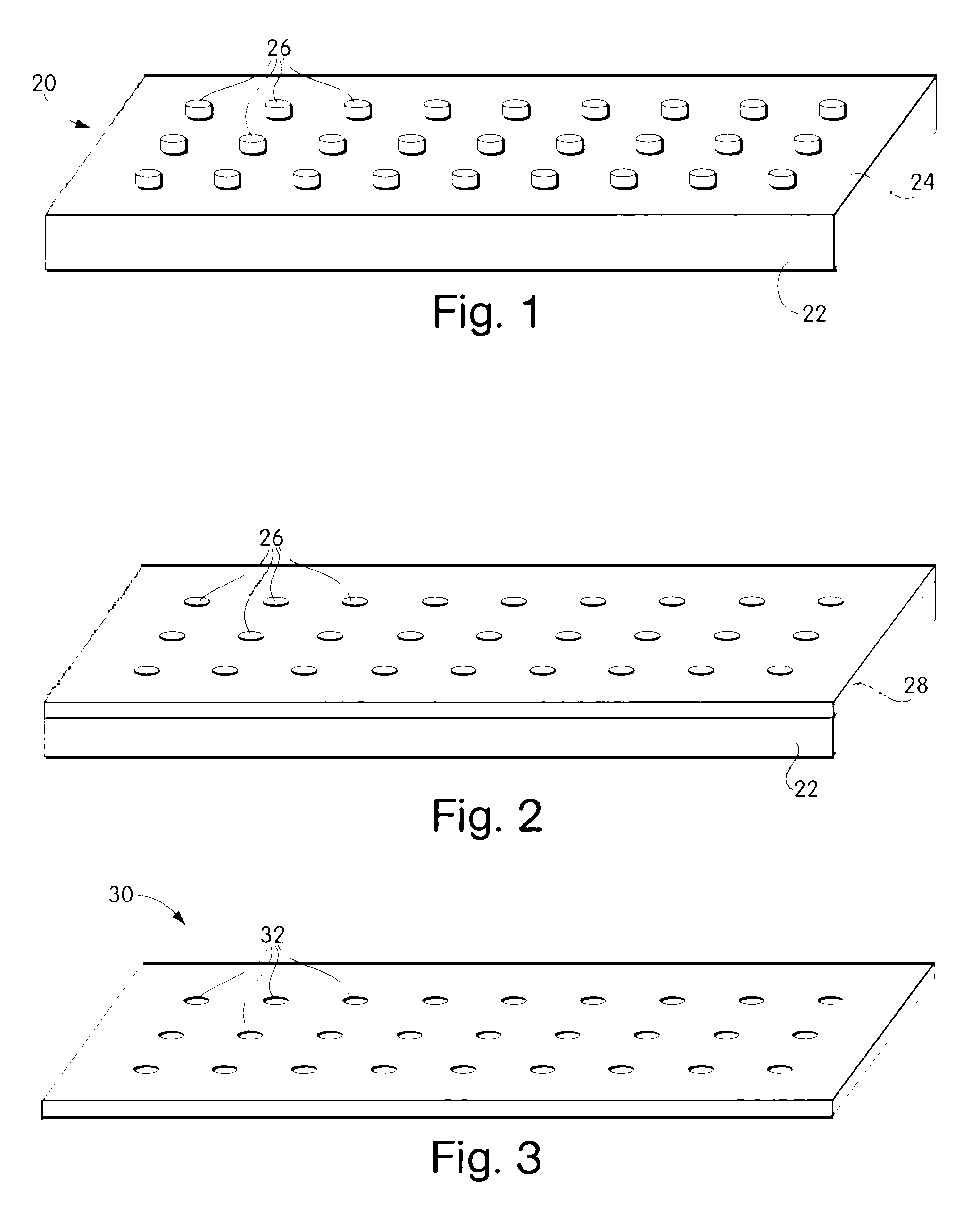
[0090]A master (FIG. 1) including an array of photoresist posts on a silicon wafer was created by photolithography. The master consisted of an array of features in photoresist created on a silicon wafer. It was generated either by “rapid prototyping” (for feature sizes>50 μm)—by using a high-resolution transparency as the photomask for photolithography—or by performing standard photolithography with a chrome mask (for feature sizes50 μm). In standard photolithography techniques, SU-8 50 (SU-8 5) resist (as received from Microlithography Chemical Corp., Newton, Mass.) was used. Spin-coating the resist at 5000 rpm for 40 s (2500 rpm for 40 s) produced a film approximately 50 μm thick. After baking the resist at 105° C. for 15 min. (5 min), it was exposed to UV light for 1 min (10 s) through a mask using a Karl Suss mask aligner. Features were developed in propylene glycol methyl ether acetate (PGMEA) fr ˜5 mi...

example 2

A “Dry” Lift-Off Method: (A) Deposition of Agent Through Channels of Mask Followed by Removal of the Mask

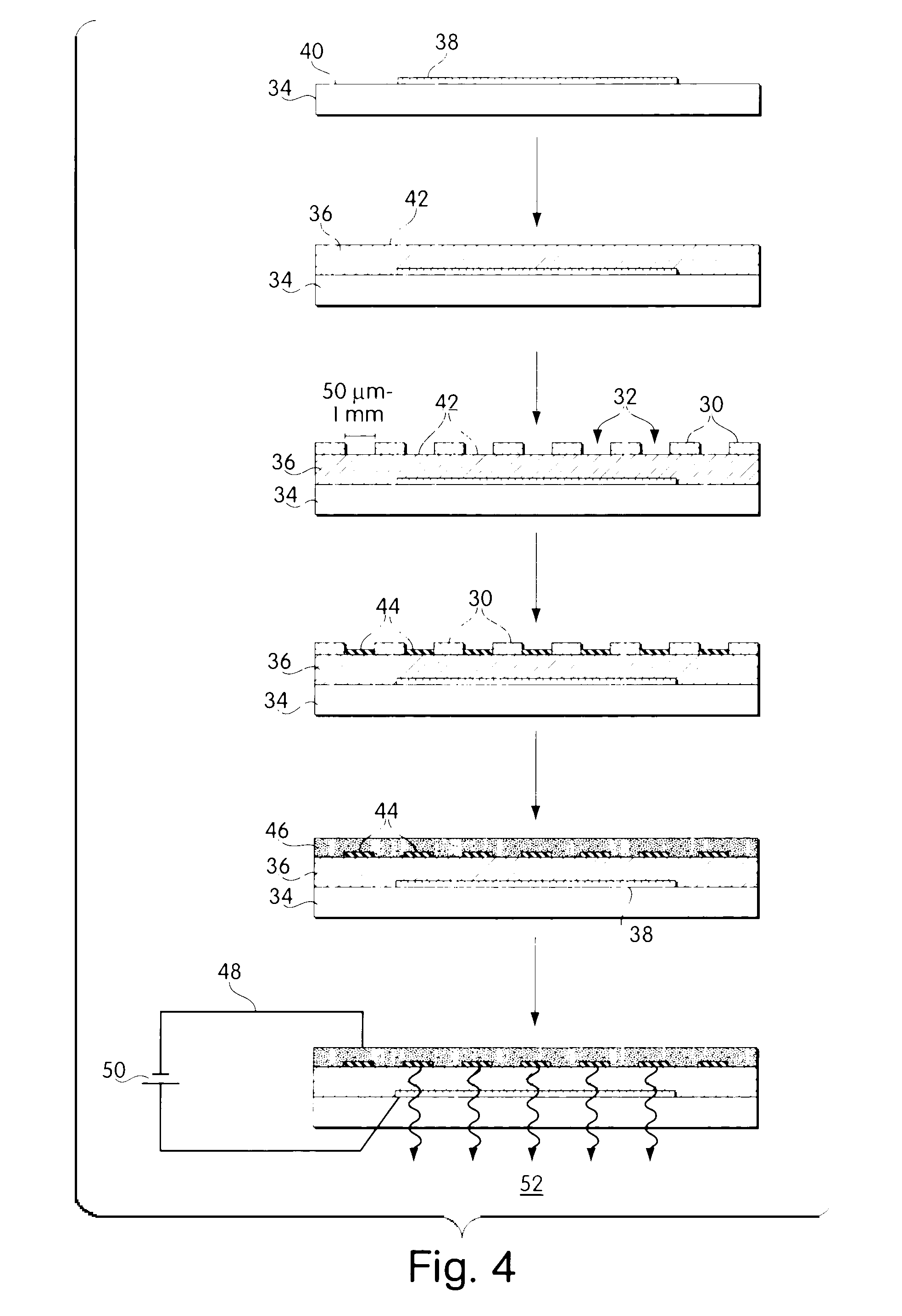
[0097]An agent was applied through the channels of the mask of Example 1 so as to form a patterned structure adhered to a substrate. A surface of the mask of Example 1 was sealed against a silicon substrate surface. The masked surface was exposed to conditions of gold e-beam deposition, resulting in deposition of gold on surfaces of the silicon substrate in register with channels of the mask. Specifically, deposition of a thin layer of titanium (5 nm. ˜0.1 nm s) followed by a layer of gold (50 nm. ˜0.3 nm s) by electron-beam evaporation (based pressure ˜5×10⁻⁷ Torr) onto the masked substrate resulted in metal on both the substrate and the mask. Instead of processing with solvents to remove the “mask” of photoresist as in conventional lift-off, a “dry” lift-off technique of the invention was carried out by simply peeling the mask from the surface and allowing the gold to remain ad...

example 3

A “Dry” Lift-Off Method: (B) Etching Through an Elastomeric Mask Followed by Removal of the Mask

[0098]As in Example 2, an agent was delivered through a mask: in this example the agent was an etchant. A PDMS mask containing circular channels of 3 microns in diameter, separated by 7 microns, was brought into conformal, sealing contact with a silicon substrate. The masked surface was then exposed to Reactive Ion Etching (RIE), i.e., SF6 gas in a plasma discharge for 8 min. The mask was then removed from the surface to reveal “wells” etched into the silicon that were in register with the channels in the PDMS mask. Patterning by RIE usually requires photolithography to create a mask followed by a wet lift-off: these two steps are bypassed by using an elastomeric mask. FIG. 10 is an SEM image of the 3 micron diameter wells in silicon. Such structures could be used as nanovials for chemical analysis of very small volumes of samples.


PUM

PropertyMeasurementUnit
thicknessaaaaaaaaaa
thicknessaaaaaaaaaa
thicknessaaaaaaaaaa

Abstract

An elastomeric mask is provided that allows deposition of a variety of materials through mask openings. The mask seals effectively against substrate surfaces, allowing simple deposition from fluid phase, gas phase, and the like or removal of material using gaseous or liquid etchants. The mask then can be simply peeled from the surface of the substrate leaving the patterned material behind. Multi-layered mask techniques are described in which openings in an upper mask allow selected openings of a lower mask to remain un-shielded, while other openings of the lower mask are shielded. A first deposition step, following by re-orientation of the upper mask to expose a different set of lower mask openings, allows selective deposition of different materials in different openings of the lower mask. Pixelated organic electroluminescent devices are provided via the described technique.

Description

RELATED APPLICATIONS[0001]This application is a continuation of International Pat. Apl. Ser. No. PCT / US99 / 08623, filed Apr. 20, 1999, which claims priority to U.S. patent application Ser. No. 09 / 063,742, filed Apr. 21, 1998, abandoned.FIELD OF THE INVENTION[0002]The present invention relates generally to surface modification, and more particularly to the deposition of material onto a surface through openings in an elastomeric mask.BACKGROUND OF THE INVENTION[0003]In fields involving microelectronic devices, sensors, and optical elements, the development of devices that are small relative to the state of the art, controllable, and conveniently and relatively inexpensively reproduced with a relatively low failure rate is important.[0004]There is currently great interest in the fabrication of optical devices based on organic materials that display electroluminescence (Burrows, et al., Current Opinion in Solid State and Materials Science, 1997, 2, 236; Baigent, et al., Synth. Meth., 199...

Claims


Application Information

Patent Timeline
Patent Type & Authority Patents(United States)
IPC IPC(8): B05D1/32B41C1/14G03F1/00G03F1/08G03F7/00G03F7/12H01L27/32H01L51/50H05B33/10
CPCB82Y10/00B82Y30/00B82Y40/00C23C14/042G03F1/00G03F7/0002G03F7/12H01L51/0011G03F7/0007H01L51/56H01L27/3211H01L27/3244H01L27/3281H10K59/35H10K59/12H10K59/17H10K71/166H10K71/00
Inventor JACKMAN, REBECCA J.DUFFY, DAVID C.WHITESIDES, GEORGE M.VAETH, KATHLEENJENSEN, KLAVS F.
Owner PRESIDENT & FELLOWS OF HARVARD COLLEGE
Why Eureka
Try Eureka