Post passivation method for semiconductor chip or wafer

a post-passivation and semiconductor chip technology, applied in the direction of semiconductor devices, semiconductor/solid-state device details, inductance, etc., can solve the problems of significantly reducing the chip performance, increasing the negative impact of the circuit performance, and increasing the capacitance of the wire, so as to improve the performance of the high-performance integrated circuit.

Inactive Publication Date: 2008-07-29
QUALCOMM INC
View PDF96 Cites 67 Cited by
  • Summary
  • Abstract
  • Description
  • Claims
  • Application Information

AI Technical Summary

Benefits of technology

[0014]It is the primary objective of the present invention to improve the performance of High Performance Integrated Circuits.
[0015]Another objective of the present invention is to reduce resistive voltage drop of the power supply lines that connect the IC to surrounding circuitry or circuit components.
[0016]Another objective of the present invention is to reduce the RC delay constant of the signal paths of high performance IC's.

Problems solved by technology

The metal connections which connect the Integrated Circuit to other circuit or system components become of relative more importance and have, with the further miniaturization of the IC, an increasingly negative impact on the circuit performance.
The parasitic capacitance and resistance of the metal interconnections increase, which degrades the chip performance significantly.
Attempts to reduce the resistance by using wider metal lines result in higher capacitance of these wires.
However, pre-testability, post-bonding visual inspection, and TCE (Temperature Coefficient of Expansion) matching to avoid solder bump fatigue are still challenges.
In mounting several packages together, such as surface mounting a ceramic package to a plastic board, the TCE mismatch can cause a large thermal stress on the solder-lead joints that can lead to joint breakage caused by solder fatigue from temperature cycling operations.

Method used


Image

  • Post passivation method for semiconductor chip or wafer
  • Post passivation method for semiconductor chip or wafer
  • Post passivation method for semiconductor chip or wafer

Examples


Embodiment Construction

[0045]The present invention teaches an Integrated Circuit structure where key re-distribution and interconnection metal layers and dielectric layers are added over a conventional IC. These re-distribution and interconnection layers allow for wider buses and reduce conventional RC delay.

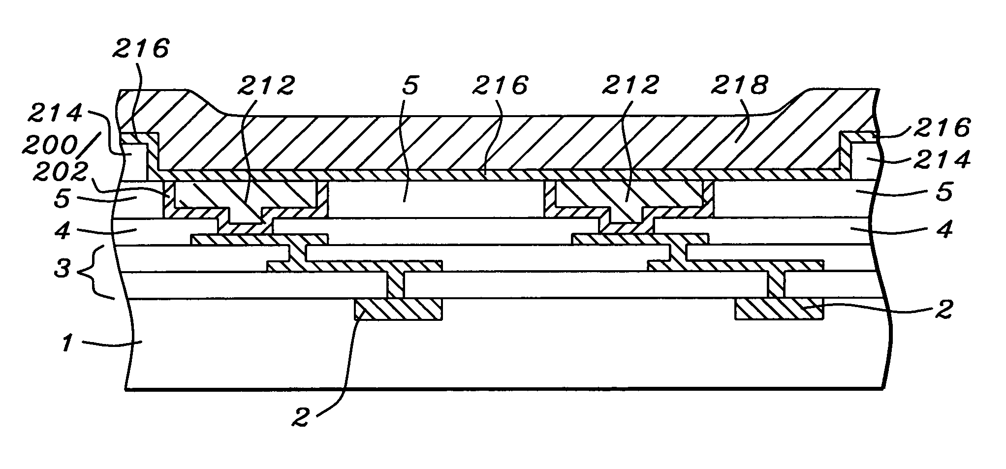
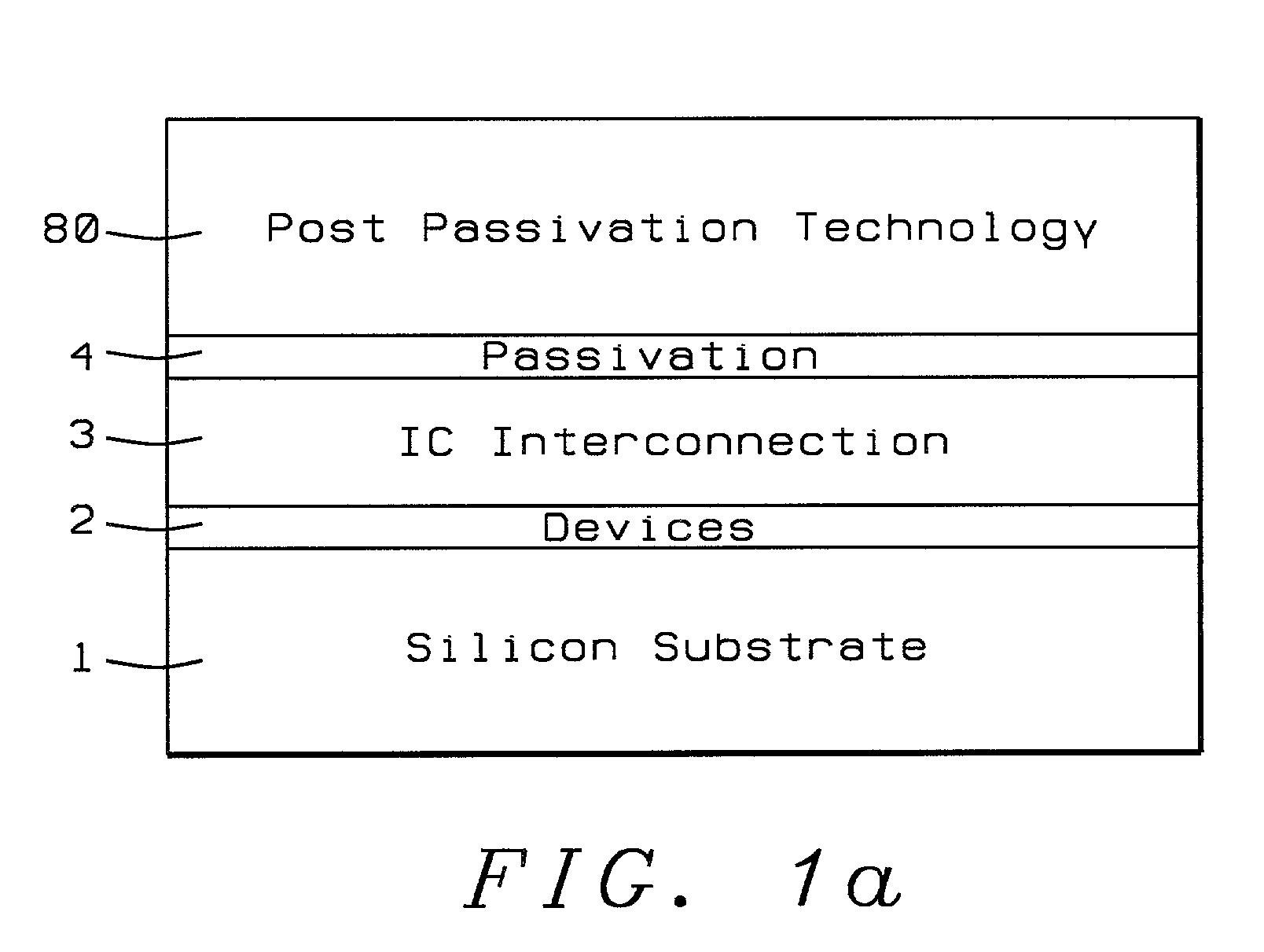
[0046]FIG. 1a shows a cross-sectional representation of a general view of the invention. Devices 2 are formed in and on a semiconductor substrate 1, and metallization is accomplished in one or more layers of IC Interconnection 3, above the device layer. The IC interconnection connects the devices to one another to form operational circuits, and also has in its top layer of metal points of electrical contact (such as bond pads), which provide connections from the IC interconnection layer to outside of the IC. A passivation layer 4 covers the IC interconnection scheme, while providing openings to the electrical contact points.

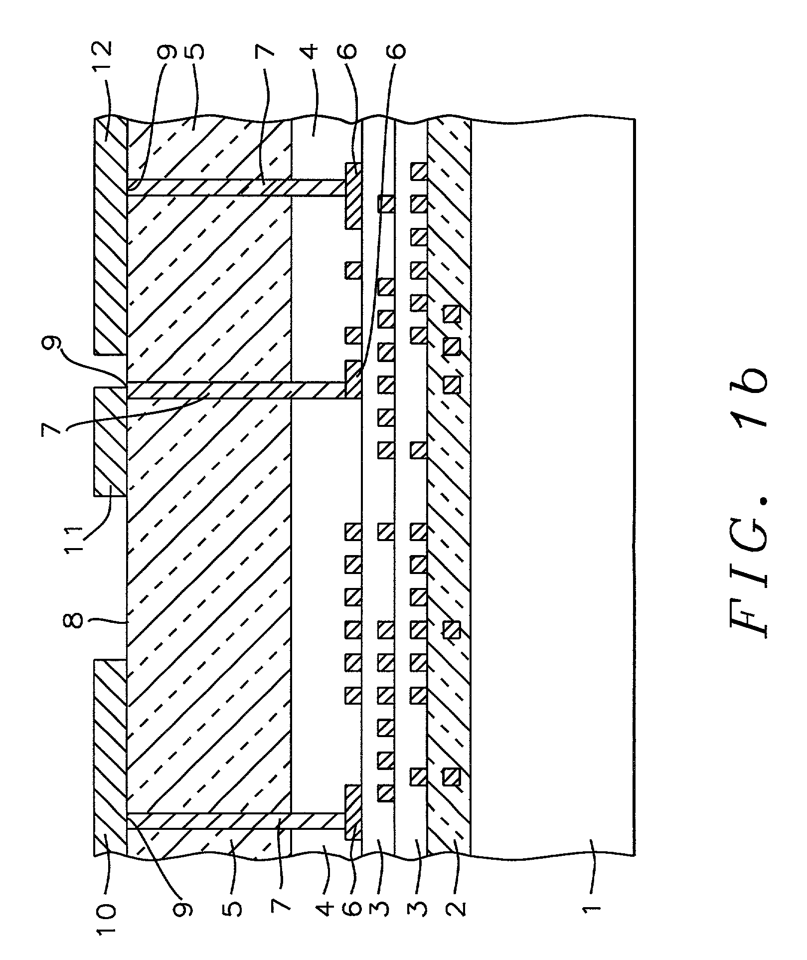
[0047]In a key aspect of the invention, the passivation openings can be as sma...


PUM


Abstract

The present invention adds one or more thick layers of polymer dielectric and one or more layers of thick, wide metal lines on top of a finished semiconductor wafer, post-passivation. The thick, wide metal lines may be used for long signal paths and can also be used for power buses or power planes, clock distribution networks, critical signal, and re-distribution of I / O pads for flip chip applications. Photoresist defined electroplating, sputter / etch, or dual and triple damascene techniques are used for forming the metal lines and via fill.

Description

[0001]This application is a continuation-in-part application of Ser. No. 10 / 058,259, filed on Jan. 29, 2002 now U.S. Pat. No. 6,620,728, which is a continuation application of Ser. No. 09 / 251,183, filed on Feb. 17, 1999, now issued as U.S. Pat. No. 6,383,916, which is a continuation-in-part application of Ser. No. 09 / 216,791, filed on Dec. 21, 1998 now abandoned.BACKGROUND OF THE INVENTION[0002](1) Field of the Invention[0003]The invention relates to the manufacturing of high performance Integrated Circuit (IC's), and more specifically to methods of achieving high performance of the Integrated Circuits by reducing the parasitic capacitance and resistance of inter-connecting wiring on chip.[0004](2) Description of the Prior Art[0005]When the geometric dimensions of the Integrated Circuits are scaled down, the cost per die is decreased while some aspects of performance are improved. The metal connections which connect the Integrated Circuit to other circuit or system components become...

Claims


Application Information

Patent Timeline
Patent Type & Authority Patents(United States)
IPC IPC(8): H01L21/4763H01L21/02H01L21/44H01L21/50H01L21/768H01L23/52H01L23/522H01L23/525H01L23/528H01L23/532H01L23/60H01L27/06H01L27/08
CPCH01L21/768H01L21/76807H01L21/76838H01L23/522H01L23/5222H01L23/5223H01L23/5225H01L23/5227H01L23/5228H01L23/525H01L23/5283H01L23/5286H01L23/5329H01L23/53295H01L23/60H01L24/11H01L24/12H01L27/0676H01L27/08H01L28/10H01L28/20H01L21/76804H01L2224/0401H01L2224/0231H01L2224/02311H01L2224/02313H01L2224/1148H01L2224/13099H01L2924/01002H01L2924/01013H01L2924/01015H01L2924/01018H01L2924/01022H01L2924/01029H01L2924/01042H01L2924/01046H01L2924/01073H01L2924/01074H01L2924/01075H01L2924/01078H01L2924/01079H01L2924/01082H01L2924/04941H01L2924/12044H01L2924/14H01L2924/15174H01L2924/15184H01L2924/15192H01L2924/15311H01L2924/19043H01L2924/30105H01L2924/30107H01L2924/3025H01L2924/01005H01L2924/01006H01L2924/01024H01L2924/01033H01L2924/014H01L2224/16225H01L2924/351H01L2924/15787H01L21/76885H01L2924/00
Inventor LIN, MOU-SHIUNGLEE, JIN-YUAN
Owner QUALCOMM INC
Why Eureka
Try Eureka