Low dielectric constant insulating material and semiconductor device using the material

a technology of low dielectric constant and insulating material, which is applied in the direction of basic electric elements, transportation and packaging, layered products, etc., can solve the problems of reducing the processing speed of ulsi, adding to the distance of wiring, and conspicuously low mechanical strength of porous siosub>2/sub>, so as to prevent the reduction of throughput speed and increase parasitic capacity

Active Publication Date: 2008-09-23
HITACHI CHEM CO LTD
View PDF8 Cites 6 Cited by
  • Summary
  • Abstract
  • Description
  • Claims
  • Application Information

AI Technical Summary

Benefits of technology

[0048]When the insulating material is used as a low dielectric interlayer insulating film for the wiring in the ULSI, the increase of the parasitic capacity between wiring layers due to the growth of the degree of integration can be suppressed and the decrease of the throughput speed can be prevented.

Problems solved by technology

It is known that this high integration results in adding to the distance of wiring.
The high integration, therefore, results in augmenting the distribution resistance and the parasitic capacity and induces a delay of signal that lowers the processing speed of ULSI.
Thus, the porous SiO2 has a conspicuously low mechanical strength as compared with the bulk SiO2 and is fragile.
When the formation of electric wires of Cu is tried by the so-called damascene process at the next step, these electric wires do not withstand the process of chemical mechanical polish (CMP) which is performed with the object of removing the excess of the Cu coat formed uniformly by the electrolytic plating, with the result that they peel or sustain a crack.
These materials have high relative dielectric constants in the range of 4.5 to 7 and have the problem of exalting the effective relative dielectric constants of respective insulating films for multilayer interconnection.
Thus, the porous SiO2 is generally brittle and vulnerable to ion impact and, therefore, encounters difficulty in forming trenches and holes in expected shapes.
An organic group-containing SiO2 does not withstand a dry etching process using ordinary perfluorocarbon (PFC) as an etching gas when the resist used in the form of film vanishes because it contain an organic group.
The organic polymer low dielectric constant materials require a hard mask because they possess compositions resembling relevant resists and fail to manifest selection ratios during dry etching to the resists.
Further, Cu is easily oxidized.
The metallic Cu allows no easy dry etching and, therefore, the feasibility of fine interconnection with the metallic Cu has been hitherto regarded as difficult.
Since the single damascene process continues to make the interconnecting layers and the interlayer connecting holes separately, it has a strong point of infallibly making them and a weak point of adding to the length of process and tending to add to the cost.
This method further suffers the technical difficulty of process to mount because of the necessity for depositing barrier films for Cu diffusion and seed Cu films without sacrificing reliability on the trenches and the via holes which are destined to have higher aspect ratios.
Though the insulating film obtained by this method excels in the flatness of the buried trenches, the publication of the patent discloses nothing about the dielectric constant.
The attempt carried out hitherto to use a low dielectric constant interlayer insulating film or Cu wiring in the ULSI multilayer interconnection has brought such problems as necessitating use of a hard mask, a barrier layer against Cu diffusion or an additional film called an etching stopper, i.e. a material possessing a high relative dielectric constant and suffering the effective relative dielectric constant of the interconnection to increase in spite of the use of a low dielectric constant interlayer insulating film having a low relative dielectric constant.

Method used


Image

  • Low dielectric constant insulating material and semiconductor device using the material
  • Low dielectric constant insulating material and semiconductor device using the material
  • Low dielectric constant insulating material and semiconductor device using the material

Examples


embodiment 1

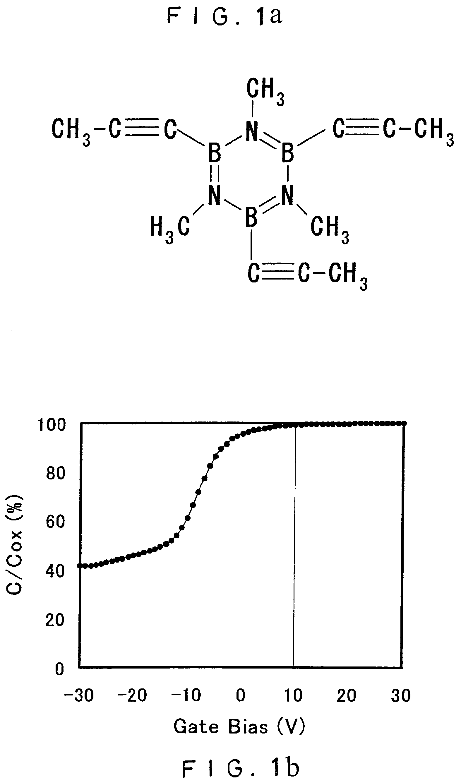
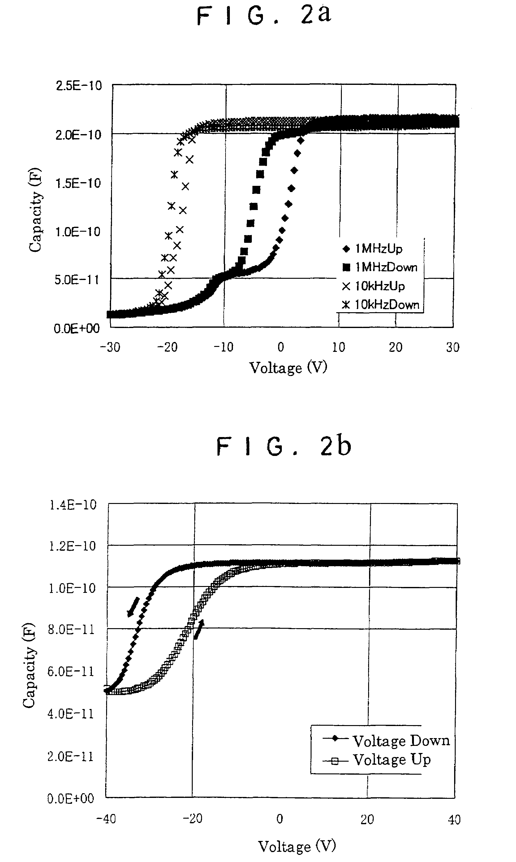
[0074]An embodiment embracing the first characteristic of this invention will be shown below. This embodiment represents a case in which a polymer similar to ethynylborazine was obtained by subjecting B,B′,B″-tripropynyl-N,N′,N″-trimethyl borazine (FIG. 1(a)) having a propynyl group linked to the boron atom of borazine to hydrosilylating polymerization with 1,3,5,7-tetramethyl cyclo-tetrasiloxane in a solvent of ethyl benzene in the presence of a platinum catalyst. The polymer solution thus obtained had a long life and could be uniformly applied to a surface with a spin coater. The thin film of polymer obtained by transforming the polymer solution to a network structure by a heat treatment was found to possess a low relative dielectric constant.

[0075]In a solvent of ethyl benzene under a nitrogen atmosphere, 1 mol of B,B′,B″-tripropynyl-N,N′,N″-trimethyl borazine having a propynyl group formed of a triple bond linked to the boron atom of borazine as a borazine derivative and 1.1 mol...

embodiment 2

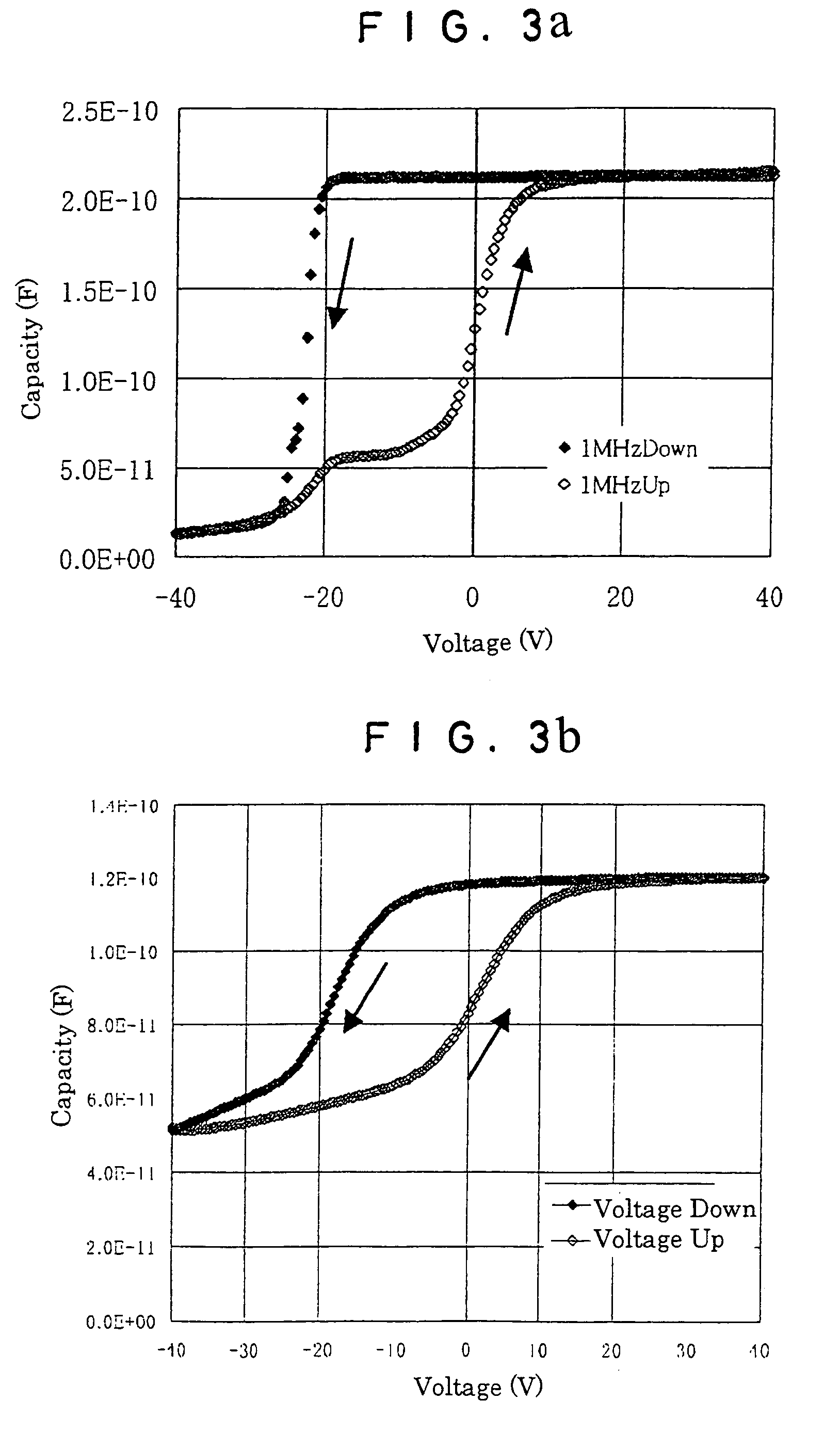
[0113]Now, Embodiment 2 that synthesized a borazine-silicone polymer by fulfilling the second characteristic of this invention will be shown below.

[0114]The borazine-siloxane polymer that is one form of the borazine-silicon polymer possesses a substituent group containing a triple bond in the boron atom of a borazine ring as shown in FIG. 4(c). It is obtained by subjecting a borazine compound possessing an alkyl substituent group in the nitrogen atom and 1,3,5,7-tetramethyl cyclosiloxane to hydrosilylating polymerizsation.

[0115]The polymerization reaction was performed in two stages. By performing the polymerization of the first stage at room temperature or 40° C., a polymer solution formed of a linear polymer uniformly soluble in a solvent was obtained. This polymer solution was applied on a Si wafer by the use of a spin coater. At the second stage, the coated wafer was heated from 200° C. through 400° C. to obtain a thin film formed of a network polymer.

[0116]The borazine-siloxane...

embodiment 3

[0152]FIG. 13 is a cross section of a semiconductor device representing Embodiment 3 of this invention. This embodiment embraces the third characteristic of this invention.

[0153]A silicon (Si) substrate 101 was separated into elements and fabricated in accordance with a prescribed circuit design to form an active device, such as a transistor. The active device, after having a BPSG / CVD-SiO2 (102) deposited thereon, connecting holes 103 opened therein for electrical connection, and a local wiring formed therein with tungsten (W), for example, and the connecting holes filled with tungsten, was treated by the chemical mechanical polishing (CMP) to have the surface thereof flattened. Denoted by 103 in the diagram are the connecting holes that were buried with W (FIG. 13(a)).

[0154]FIG. 13(a) avoids depicting details, such as the transistor, for the sake of simplicity. The following explanation will be made with reference to the part A of FIG. 13(a), which is a magnified diagram. This inve...


PUM

PropertyMeasurementUnit
temperatureaaaaaaaaaa
relative dielectric constantaaaaaaaaaa
dielectric constantaaaaaaaaaa

Abstract

The use of a material possessing a six-member borazine ring consisting of at least boron and nitrogen elements in the form of a low dielectric constant insulating film in a hard mask, a Cu diffusion barrier layer and an etching stopper which are necessary when low dielectric constant interlayer insulating films and Cu wiring in the multilayer interconnection of an LSI allows the parasitic capacity between the multilayer wirings to be suppressed and enables the ULSI to produce a high-speed operation.

Description

BACKGROUND OF THE INVENTION[0001]1. Field of the Invention[0002]This invention relates to a low dielectric constant insulating material to be used as an interlayer insulating film for multilayer interconnection in an integrated circuit and a semiconductor device using the material.[0003]2. Description of the Prior Art[0004]The demand for further integration of ultra large-scale integrated (ULSI) circuits has been continuing to mount. This high integration requires the electric wires to be disposed densely by narrowing the intervals between the adjacent electric wires and also requires the electric wires to thin and fit multilayer disposition. It is known that this high integration results in adding to the distance of wiring. The high integration, therefore, results in augmenting the distribution resistance and the parasitic capacity and induces a delay of signal that lowers the processing speed of ULSI. Thus, the solution of these defects constitutes an important task.[0005]For the ...

Claims


Application Information

Patent Timeline
Patent Type & Authority Patents(United States)
IPC IPC(8): B32B9/04C08G77/56C08G77/48C08G79/08C08G77/60H01L21/312H01L21/318H01L21/768H01L23/522
CPCC08G77/56C08G77/60C08G79/08H01L21/318H01L21/76801H01L21/76835H01L21/76813H01L21/76829H01L21/76832H01L21/76807H01L21/76834Y10T428/31663H01L21/02123H01L21/02118H01L21/02211
Inventor UCHIMARU, YUKOINOUE, MASAMI
Owner HITACHI CHEM CO LTD
Why Eureka
Try Eureka