Doped nanoparticle semiconductor charge transport layer

a technology of charge transport layer and doped nanoparticle, which is applied in the direction of semiconductor devices, crystal growth process, chemistry apparatus and processes, etc., can solve the problems of insufficient device performance for market needs, relatively high cost, and limited efficiency, and achieves low cost, limit the usefulness of these devices, and simple forming method

Inactive Publication Date: 2009-02-24
EASTMAN KODAK CO
View PDF3 Cites 11 Cited by
  • Summary
  • Abstract
  • Description
  • Claims
  • Application Information

AI Technical Summary

Benefits of technology

[0017]It is an advantage of the present invention to enable a simple method of forming doped semiconductor nanoparticles. The semiconductor nanoparticles are doped in-situ with dopant materials during the process of synthetic growth of the colloidal nanoparticles. Inorganic device layers composed of inorganic nanoparticles are typically highly resistive, which limits the usefulness of these devices despite their low cost. By incorporating in-situ doped inorganic nanoparticles into the transport layers of devices, one can produce the devices at low cost while still maintaining good device performance. In addition, separate thermal anneal steps are used to reduce the resistivities of the charge transport layers. Doped transport layers help device performance by increasing the separation of the n- and p-quasi Fermi levels, reduce ohmic heating, and aide in forming ohmic contacts. By forming the transport layers from in-situ doped inorganic nanoparticles, the device layers can be deposited by low cost processes, such as, drop casting, spin coating, or inkjetting. The resulting nanoparticle-based device can also be formed on a range of substrates.
to enable a simple method of forming doped semiconductor nanoparticles. The semiconductor nanoparticles are doped in-situ with dopant materials during the process of synthetic growth of the colloidal nanoparticles. Inorganic device layers composed of inorganic nanoparticles are typically highly resistive, which limits the usefulness of these devices despite their low cost. By incorporating in-situ doped inorganic nanoparticles into the transport layers of devices, one can produce the devices at low cost while still maintaining good device performance. In addition, separate thermal anneal steps are used to reduce the resistivities of the charge transport layers. Doped transport layers help device performance by increasing the separation of the n- and p-quasi Fermi levels, reduce ohmic heating, and aide in forming ohmic contacts. By forming the transport layers from in-situ doped inorganic nanoparticles, the device layers can be deposited by low cost processes, such as, drop casting, spin coating, or inkjetting. The resulting nanoparticle-based device can also be formed on a range of substrates.

Problems solved by technology

Most semiconductor devices in use today, both inorganic and organic, are in part or completely formed using expensive vacuum deposition processes.
There are ongoing efforts to find a low cost manufacturing process, but to date, device performance has been inadequate for market needs.
While these devices are useful in certain applications, their efficiency has been somewhat limited, yielding conversion efficiencies, e.g., solar power to electrical power, of typically marginally better than 10-20%.
Although efficiencies of these devices have been improving through costly improvements to device structure, the relative inefficiency of these devices, combined with their relatively high cost, have combined to inhibit the widespread adoption of solar electricity in the consumer markets.
However, the performance of these devices were not reported, and the conductivity of such a mixed photoactive layer is expected to be low due to the high resistivity of the polymeric binder.
A large part of the low efficiency was undoubtedly due to the films being insulators (even after sintering) due to the lack of doping.
In addition, the process is inefficient with respect to usage of its starting materials.
As a result of surface plasmon effects (K. B. Kahen, Appl. Phys. Lett. 78, 1649 (2001)), having metal layers adjacent to emitter layers results in a loss emitter efficiency.
As is well known in the art, highly doping wide bandgap semiconductors is difficult as a result of self-compensation effects.
Consequently, forming ohmic contacts to these layers can prove to be difficult.
The dominant ones are high manufacturing costs, difficulty in combining multi-color output from the same chip, and the need for high cost and rigid substrates.
However, many of these dopants are unstable and the resistivities are many orders of magnitude higher than crystalline LED values of ˜0.1 ohm-cm.
The result of employing resistive layers is that one suffers from ohmic heating effects; it is difficult to make ohmic contacts; and since the drive current of the device is limited, so is the overall brightness of the device.
The above examples illustrate that higher performance semiconductor devices can be created from crystalline semiconductor materials; but with the drawback of high manufacturing costs.
Attempts to reduce the manufacturing costs by employing organic materials result in lower performance devices whose specs sometimes fall significantly short of market requirements (e.g., organic-based photovoltaics).
Two approaches to lower the cost of crystalline semiconductor materials are to employ either amorphous or polycrystalline inorganic semiconductor materials; however, both of these approaches have well-known drawbacks.
Taking the case of devices formed from amorphous Si, both thin-film transistor and photovoltaic (PV) devices have significantly reduced performance due to low mobilities (and the Staebler-Wronski effect for PVs).
However, sputtering is a higher cost, vacuum-based deposition process and CBD, though chemically based, has long deposition times and is inefficient in its usage of starting materials, as stated previously.

Method used


Image

  • Doped nanoparticle semiconductor charge transport layer
  • Doped nanoparticle semiconductor charge transport layer
  • Doped nanoparticle semiconductor charge transport layer

Examples


example 1

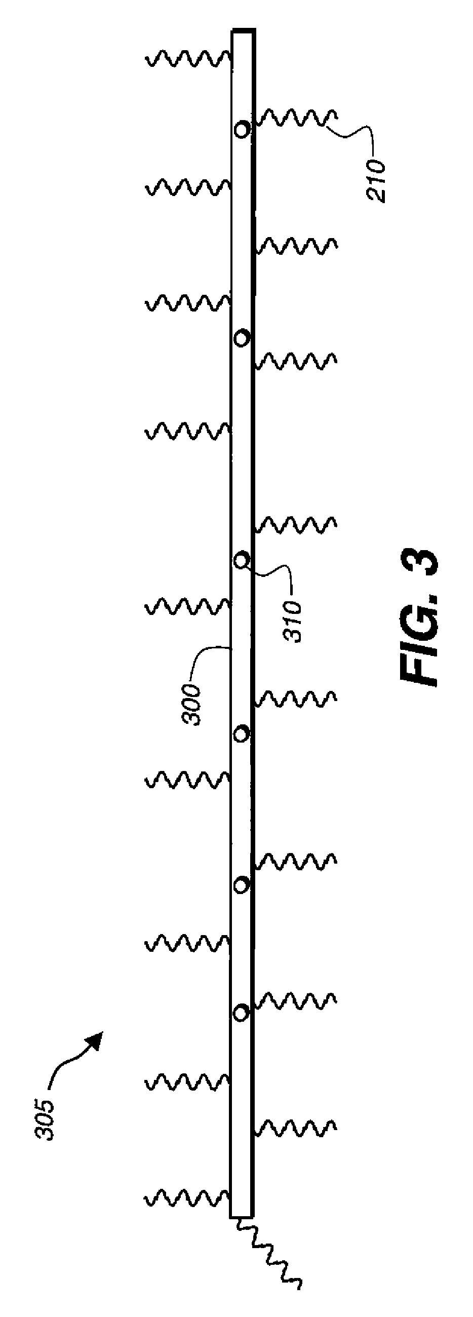
[0034]Doped and undoped semiconductor transport layers were formed on glass substrates. The test system was CdSe, with and without In doping (a donor for CdSe which substitutes on the cation site). Undoped CdSe quantum wires 300 were formed by a procedure analogous to that by Pradhan et al. (N. Pradhan et al., Nano Letters 6, 720 (2006)). In our version the cadmium precursor is cadmium acetate and the Se precursor is selenourea, where equal molar (1.27×10⁻⁴ moles) amounts are used in the synthesis. The coordinating solvent for the growth is octylamine (OA), which is degassed at 30° C. for 30 minutes prior to its usage. In a small vial inside of a dry box, 0.03 g of cadmium acetate is added to 4 ml OA. After gently heating this mixture under constant spinning, the solution goes clear in 5-10 minutes. Next this mixture is placed in a three-neck flask and placed on a Schlenk line. At room temperature, the contents are subjected to three cycles of evacuation, followed by argon refilling...


PUM

PropertyMeasurementUnit
temperaturesaaaaaaaaaa
temperatureaaaaaaaaaa

Abstract

A method is disclosed for making a doped semiconductor transport layer for use in an electronic device comprising: growing in-situ doped semiconductor nanoparticles in a colloidal solution; depositing the in-situ doped semiconductor nanoparticles on a surface; and annealing the deposited in-situ doped semiconductor nanoparticles so that the organic ligands boil off the surface of the in-situ doped semiconductor nanoparticles.

Description

FIELD OF THE INVENTION[0001]The present invention relates to inorganic semiconductor devices that include charge transport layers composed of inorganic nanoparticles.BACKGROUND OF THE INVENTION[0002]Charge transport layers containing n-type or p-type semiconductors can be used in making a variety of devices such as field effect transistors, bipolar transistors, p-n diodes, light emitting diodes (LEDs), lasers, sensors, solar cells and others. Most semiconductor devices in use today, both inorganic and organic, are in part or completely formed using expensive vacuum deposition processes. There are ongoing efforts to find a low cost manufacturing process, but to date, device performance has been inadequate for market needs. Therefore, there is a need for a low cost technique of forming high quality inorganic charge transport layers for use in semiconductor devices.[0003]In general, both n-type and p-type materials can be referred to as charge transport materials, and the layers of a d...

Claims


Application Information

Patent Timeline
Patent Type & Authority Patents(United States)
IPC IPC(8): H01L21/00
CPCH01L21/02521H01L21/02601H01L21/02628Y10S977/892
Inventor KAHEN, KEITH B.
Owner EASTMAN KODAK CO
Why Eureka
Try Eureka