Printed wiring board having a roughened surface formed on a metal layer, and method for producing the same
a metal layer and rough surface technology, applied in the direction of conductive pattern formation, dielectric characteristics, and insulating substrate metal adhesion improvement, can solve the problems of low fracture toughness of -level resin isolating layer, signal conduction noise tends to occur, and achieve good mechanical properties, good mechanical properties, and good mechanical properties
- Summary
- Abstract
- Description
- Claims
- Application Information
AI Technical Summary
Benefits of technology
Problems solved by technology
Method used
Image
Examples
example 1
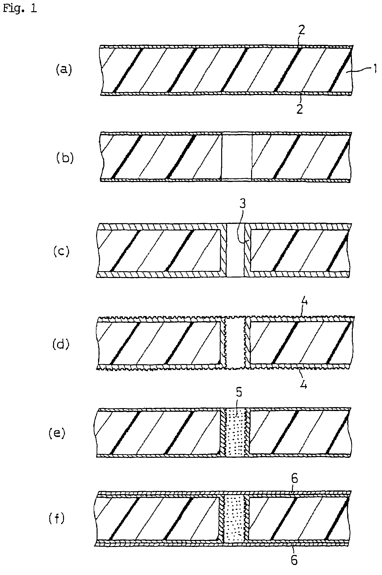
[0683](1) A copper-clad BT resin laminate (Mitsubishi Gas Chemical; product designation: HL 830-C, 8T12D) comprising a 0.8 mm-thick BT [bis(maleimide)triazine] resin substrate 1 and an 18 μm-thick copper foil 2 laminated to both sides thereof was used as the starting material [FIG. 1(a)]. First, this copper-clad laminate was drilled [FIG. 1(b)] and a palladium-tin coloid was applied. Using an aqueous electroless plating solution of the under-mentioned formulation, electroless plating was performed to form a 0.7 μm-thick electroless plated copper film on the entire substrate surface.
[0684]
[Aqueous electroless plating solution]EDTA 150 g / LCopper sulfate 20 g / LHCHO 30 ml / LNaOH 40 g / Lα,α′-Bipyridyl 80 mg / LPEG 0.1 g / L[Electroless plating conditions]Bath temperature:70° C., for 30 min.
[0685]Then, using an aqueous electroplating solution of the under-mentioned formulation, copper electroplating was performed to provide a 15 μm-thick copper electrodeposition film [FIG. 1(c)].
[0686]
[Aque...
example 2
[0704]In this example, Mitsui Chemical's TPX (product designation) was used as polyolefin resin and desmear treatment and surface modification were carried out by oxygen plasma treatment. After this surface modification, the presence of polar groups such as hydroxyl and carbonyl on the surface of the insulating layer was confirmed.
[0705]Except for the above modification and further except that Ni was deposited on the polyolefin resin insulating layer under the conditions of gas pressure: 0.6 Pa, temperature: 100° C., power: 200 W and time: 1 min, the procedure of Example 1 was otherwise repeated to manufacture a multilayer printed circuit board.
example 3
[0706]In this example, Idemitsu Petrochemical's SPS (product designation) was used as polyolefin resin and desmear tratment and surface modification by oxygen plasma treatment was carried out. After this surface modification, the presence of polar groups such as hydroxyl and carbonyl on the surface of the insulating layer was confirmed.
[0707]Except for the above modification and further except that Pt was deposited on the polyolefin resin insulating layer under the conditions of gas pressure: 0.6 Pa, temperature: 100° C., power: 200 W and time 2 min, the procedure of Example 1 was otherwise repeated to manufacture a multilayer printed circuit board.
PUM
| Property | Measurement | Unit |
|---|---|---|
| melting points | aaaaa | aaaaa |
| melting points | aaaaa | aaaaa |
| pore diameter | aaaaa | aaaaa |
Abstract
Description
Claims
Application Information


