Printed wiring board and method for producing the same

a printed circuit board and wiring board technology, applied in the direction of conductive pattern formation, dielectric characteristics, and insulating substrate metal adhesion improvement, can solve the problems of low fracture toughness of the -level resin isolating layer, signal conduction noise tends to occur, and achieves good mechanical properties, good mechanical properties, and good mechanical properties.

Inactive Publication Date: 2005-11-24
IBIDEN CO LTD
View PDF35 Cites 83 Cited by
  • Summary
  • Abstract
  • Description
  • Claims
  • Application Information

AI Technical Summary

Benefits of technology

[0033] Accomplished in view of the above state of the art, the present invention has for its object to provide a multilayer printed circuit board which is very satisfactory in fracture toughness, dielectric constant, adhesion and processability, among other characteristics.

Problems solved by technology

When the surfaces of the interlayer resin insulating layer and conductor circuit are roughened so as to insure good adhesion as in the above conventional manufacturing process, the carrying of high frequency signals results in that the signals selectively travel in the surface of the roughed layer of the conductor circuit owing to a skin effect and the problem of signal conduction noise tends to occur on account of the surface irregularities.
Furthermore, the epoxy acrylate resin which is generally used for inter-level resin isolating layer is low in fracture toughness and circuit boards using this resin tends to undergo cracking across the interface between the conductor circuit and the resin insulating layer under the conditions of the heat cycle test.
Moreover, when the multilayer printed circuit board is one employing fluororesin as the material for interlayer resin insulating layers, while the fluororesin has low dielectric constant, low hygroscopicity and high in fracture toughness, the substrate board must be heated to a temperature close to 350° C. in the pressure-laminating stage for construction of an interlayer resin insulating layer but any printed circuit board which has experienced such a high-temperature environment tends to undergo early aging.
However, multilayer printed circuit boards at the product level are not uniform in the density of conductor circuits so that it is difficult to completely cover the rough Cu—Ni—P acicular alloy layer with a Sn layer and thereby prevent dissolution of the conductor circuit.
Furthermore, when the plating of the conductor circuit with Cu—Ni—P acicular alloy is repeated and the plating bath is degraded, the problem occurred that the plating metal can hardly be deposited effectively on the conductor circuit.
Furthermore, as mentioned above, when the roughening treatment is applied to the conductor circuit, signals are carried selectively by the superficial portion of the conductor circuit so that the signal delay is sometimes induced by the surface irregularities.
This trouble is particularly pronounced when the substrate is a resin board which is lower in dielectric constant and dielectric loss tangent than a ceramic board.
Furthermore, a resin board is poor in heat radiation factor as compared with a metal or ceramic board and, hence, liable to accumulate heat, with the result that the ion diffusion rate of the copper constituting the conductor circuit is high and this ion migration tends to destroy the layer to layer insulation.
However, this is a technology for building up conductor circuits and interlayer resin insulating layers chiefly on one side of a substrate board and unlike the case of using a ceramic board or a metal road, the resin substrate board cannot inhibit shrinkage and expansion of the interlayer resin insulating layer to occur warps and cracks which are sometimes induced across the interface between the interlayer resin insulating layer and the conductor circuit.
Furthermore, when an attempt is actually made to construct a conductor circuit by using this technique, there is sometimes encountered the trouble that the conductor circuit peels from the metal layer composed of, for example, chromium, nickel or titanium.
Thus, when a metal layer is formed on the surface of a resin insulating layer by a physical vapor deposition technique, the metal layer exposed to a high deposition temperature is oxidized on the surface so that when a conductor circuit is formed directly on the oxidized surface, the interposition of the oxide layer between the metal layer and the conductor circuit weakens the adhesion so that the conductor circuit tends to peel off.
Moreover, even if the metal layer is formed by a chemical vapor deposition technique or by plating, said surface oxidation occurs when the substrate board is allowed to sit in the air, so that the conductor circuit tends to peel off.
The use of a metal forming a passivation layer, such as Ni or Al, in the construction of said metal layer is disadvantageous in that etching with a rather easily manageable acid such as hydrochloric acid or sulfuric acid cannot proceed smoothly because the oxide once formed in the course of etching is not readily decomposed by the above-mentioned acid.
Furthermore, when an oxide film has been formed on the surface of such a metal layer, it is no longer easy to remove it by etching.
In addition, those metals are soluble in strong acid such as concentrated nitric acid and aqua regia and, therefore, can be etched with an etching solution based on concentrated nitric acid or a cyanide or fluoride solution but because these acids are toxic and violent substances not easy to handle, the process control is difficult and the work environment tends to be adversely affected.
However, if, in the conventional manufacturing process for a multilayer printed circuit board, an electroless plated nickel film is formed on an electroplated film and, then, a roughened layer of Cu—Ni—P alloy is superimposed, the adhesion between the plated nickel film and a roughened layer of Cu—Ni—P alloy, which is usually high in adhesion, will be unexpectedly low so that the roughened layer of Cu—Ni—P alloy tends to be exfoliated from the plated nickel layer.
There also is the problem that, in the step of plating the conductor circuit with Cu—Ni—P alloy, the plating bath is progressively degraded because of repeated use thereof so that the plating metal will not be deposited neatly on the surface of the conductor circuit.
Moreover, in order to form a cover metal layer, e.g. an Sn layer, in the above process for manufacting a multilayer printed circuit board, the conductor circuit having a roughened surface must be electroless plated but this introduces complexity to the production process and leads to increased costs of production.
Moreover, when via holes are formed on such a conductor circuit having a cover metal layer, e.g. an Sn layer, a delamination trouble may take place in the areas of contact between the via holes and the underlying conductor circuit under the conditions of heating or the heat cycle test, thus reducing the connection reliability of the via holes.

Method used


Image

  • Printed wiring board and method for producing the same
  • Printed wiring board and method for producing the same
  • Printed wiring board and method for producing the same

Examples


example 1

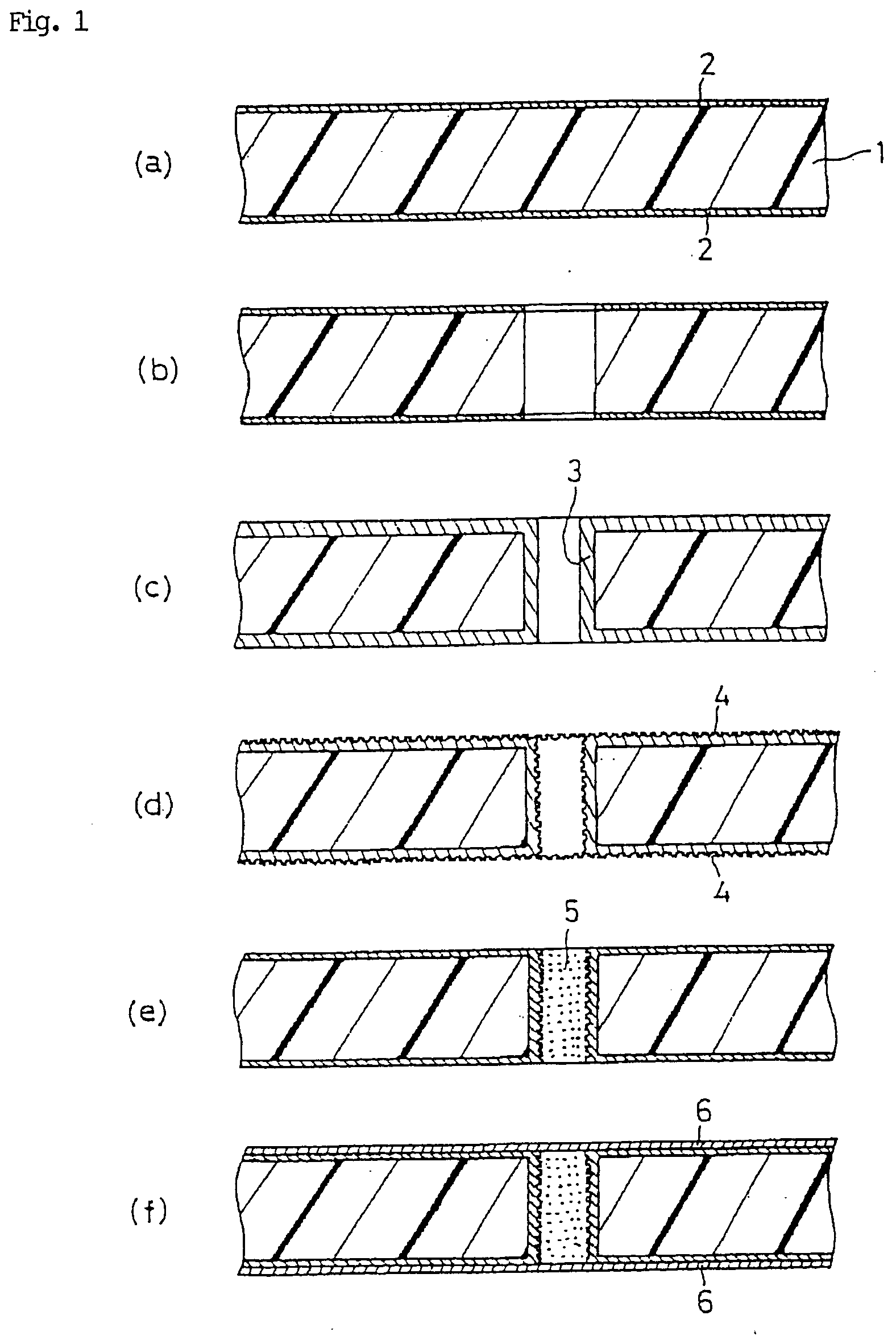
[0675] (1) A copper-clad BT resin laminate (Mitsubishi Gas Chemical; product designation: HL 830-C, 8T12D) comprising a 0.8 mm-thick BT [bis(maleimide)triazine] resin substrate 1 and an 18 μm-thick copper foil 2 laminated to both sides thereof was used as the starting material [FIG. 1(a)]. First, this copper-clad laminate was drilled [FIG. 1(b)] and a palladium-tin coloid was applied. Using an aqueous electroless plating solution of the under-mentioned formulation, electroless plating was performed to form a 0.7 μm-thick electroless plated copper film on the entire substrate surface.

[Aqueous electroless plating solution]EDTA 150 g / LCopper sulfate  20 g / LHCHO  30 ml / LNaOH  40 g / Lα,α′-Bipyridyl  80 mg / LPEG 0.1 g / L[Electroless plating conditions]Bath temperature:70° C., for 30 min.

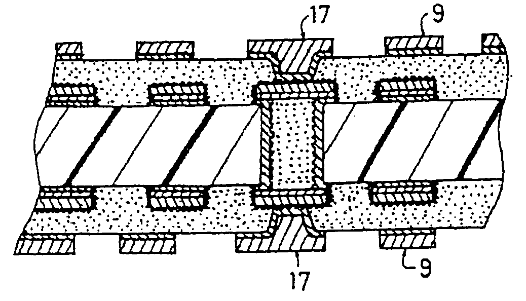
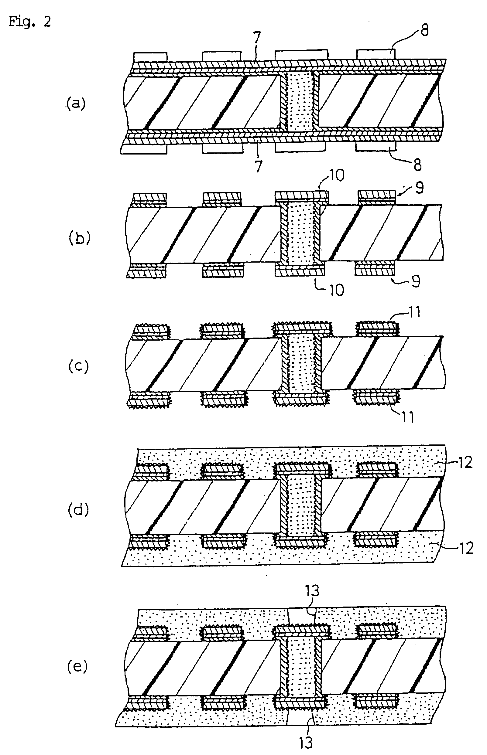
[0676] Then, using an aqueous electroplating solution of the under-mentioned formulation, copper electroplating was performed to provide a 15 μm-thick copper electrodeposition film [FIG. 1(c)].

[Aqueous el...

example 2

[0693] In this example, Mitsui Chemical's TPX (product designation) was used as polyolefin resin and desmear treatment and surface modification were carried out by oxygen plasma treatment. After this surface modification, the presence of polar groups such as hydroxyl and carbonyl on the surface of the insulating layer was confirmed.

[0694] Except for the above modification and further except that Ni was deposited on the polyolefin resin insulating layer under the conditions of gas pressure: 0.6 Pa, temperature: 100° C., power: 200 W and time: 1 min, the procedure of Example 1 was otherwise repeated to manufacture a multilayer printed circuit board.

example 3

[0695] In this example, Idemitsu Petrochemical's SPS (product designation) was used as polyolefin resin and desmear tratment and surface modification by oxygen plasma treatment was carried out. After this surface modification, the presence of polar groups such as hydroxyl and carbonyl on the surface of the insulating layer was confirmed.

[0696] Except for the above modification and further except that Pt was deposited on the polyolefin resin insulating layer under the conditions of gas pressure: 0.6 Pa, temperature: 100° C., power: 200 W and time 2 min, the procedure of Example 1 was otherwise repeated to manufacture a multilayer printed circuit board.


PUM

PropertyMeasurementUnit
toughnessaaaaaaaaaa
dielectric constantaaaaaaaaaa
adhesionaaaaaaaaaa

Abstract

The present invention has for its object to provide a multilayer printed circuit board which is very satisfactory in facture toughness, dielectric constant, adhesion and processability, among other characteristics. The present invention is directed to a multilayer printed circuit board comprising a substrate board, a resin insulating layer formed on said board and a conductor circuit constructed on said resin insulating layer, wherein said resin insulating layer comprises a polyolefin resin.

Description

CROSS REFERENCE TO RELATED APPLICATIONS [0001] This is a divisional of U.S. application Ser. No. 09 / 806,203 filed Mar. 27, 2001, which is a §371 of PCT Application No. PCT / JP99 / 05266 filed Sep. 28, 1999, the disclosure of which is incorporated herein by reference in its entirety.TECHNICAL FIELD [0002] The present invention relates to a printed circuit board and a technology for producing said printed circuit board. BACKGROUND ART [0003] With the recent trend toward ever higher frequencies of signals, package board materials are required to be of low dielectric constant and low dielectric loss tangent. Therefore, the current mainstream of package board material is shifting from ceramics to resins. [0004] More recently, since higher wiring densities are also required and the printed circuit board known as the multilayer buildup printed circuit board comprising a plurality of circuit layers is getting a more dominant position. [0005] The multilayer printed circuit board called the mult...

Claims


Application Information

Patent Timeline
Patent Type & Authority Applications(United States)
IPC IPC(8): C23G1/10H05K3/00H05K3/06H05K3/10H05K3/38H05K3/46
CPCC23G1/10Y10T29/49124H05K3/062H05K3/067H05K3/108H05K3/384H05K3/385H05K3/388H05K3/4602H05K3/4644H05K3/4661H05K2201/0129H05K2201/0158H05K2201/0338H05K2201/09563H05K2201/0959H05K2201/096H05K2203/0307H05K2203/0315H05K2203/072H05K2203/1105H01L2924/0002H05K3/0094Y10T29/49151Y10T29/49165Y10T29/49155Y10T29/49163Y10T428/24917H01L2924/00H05K3/46
Inventor EN, HONCHINHAYASHI, MASAYUKIWANG, DONGDONGSHIMADA, KENICHIASAI, MOTOOSEKINE, KOJINAKAI, TOHRUICHIKAWA, SHINICHIROTOYODA, YUKIHIKO
Owner IBIDEN CO LTD
Why Eureka
Try Eureka