However, the organic photoreceptor is liable to be abraded when repeatedly used, which causes deterioration of the charge potential and
photosensitivity thereof and damages of the surface thereof, resulting in background
fouling and deterioration of
image density of the
resultant images.
However, any of these conventional technologies are insufficient in terms of simultaneous pursuit of higher-quality image and higher durability.
Although the dispersibility can be improved with a dispersant, light tends to scatter because the
resultant coated layer has a small flexibility, resulting in deterioration of latent images and production of blurred images.
A photoreceptor using the (1) hardening binder tends to increase the residual potential and produce images having low
image density because of poor compatibility of the hardening binder with a charge transport material and impurities such as a
polymerization initiator and an unreacted residue.
A photoreceptor using the (2) charge transport
polymer material has good abrasion resistance, but does not have satisfactory durability.
In addition, the charge transport
polymer material is difficult to polymerize and purify, and a
coating liquid including the charge transport polymer material has high
viscosity.
In addition, when the
inorganic filler and a binder resin form large concavities and convexities on the surface of the photoreceptor, the
cleanability hereof deteriorates, resulting in toner filming and distorted images.
These technologies of (1), (2) and (3) do not fully satisfy an overall durability including electrical durability, mechanical durability and image durability required for an organic photoreceptor.
However, although disclosing that a
protection layer thereof includes the hardened polyfunctional
acrylate monomer, Japanese Patent No. 3262488 only discloses that a charge transport material may be included therein and does not disclose specific examples thereof.
In addition, when a low-molecular-weight charge transport material is simply included in a
surface layer, the low-molecular-weight charge transport material is not soluble with the hardened polyfunctional
acrylate monomer and the low-molecular-weight charge transport material separates out and becomes cloud in the
surface layer, and which causes deterioration of
mechanical strength of the resultant photoreceptor.
Further, since the hardened polyfunctional
acrylate monomer is reacted in a
surface layer including a polymer binder, a three-dimensional network is not
fully developed therein and the crosslinking
bond density is thin, and therefore the photoreceptor does not have noticeable abrasion resistance.
The photoreceptor has both good abrasion resistance and electrical property, but when the binder resin not having a reactivity with a charge transport material is used, the binder resin has poor compatibility with a hardened material produced by a reaction between the monomer and charge transport material and the crosslinked transport layer has a layer separation therein, and which occasionally causes damages, and adherence of an external additive in a toner and a paper
powder on the surface of the photoreceptor.
As mentioned, above, a three-dimensional network is not
fully developed therein and the crosslinking
bond density is thin, and therefore the photoreceptor does not have noticeable abrasion resistance.
In addition, the monomer is
bifunctional, which is unsatisfactory in terms of the abrasion resistance.
Therefore, the resultant photoreceptor does not have a sufficient crosslinking density, and the electrical and property and the abrasion resistance thereof are not satisfactory.
Although having a high
hardness because of its high crosslinking
bond density, the photosensitive layer includes a bulky positive hole transport material having two or more chain polymeric functional groups, and a
distortion appears in the hardened compound and an
internal stress increases to cause a crack on the crosslinked surface layer and a peeling thereof.
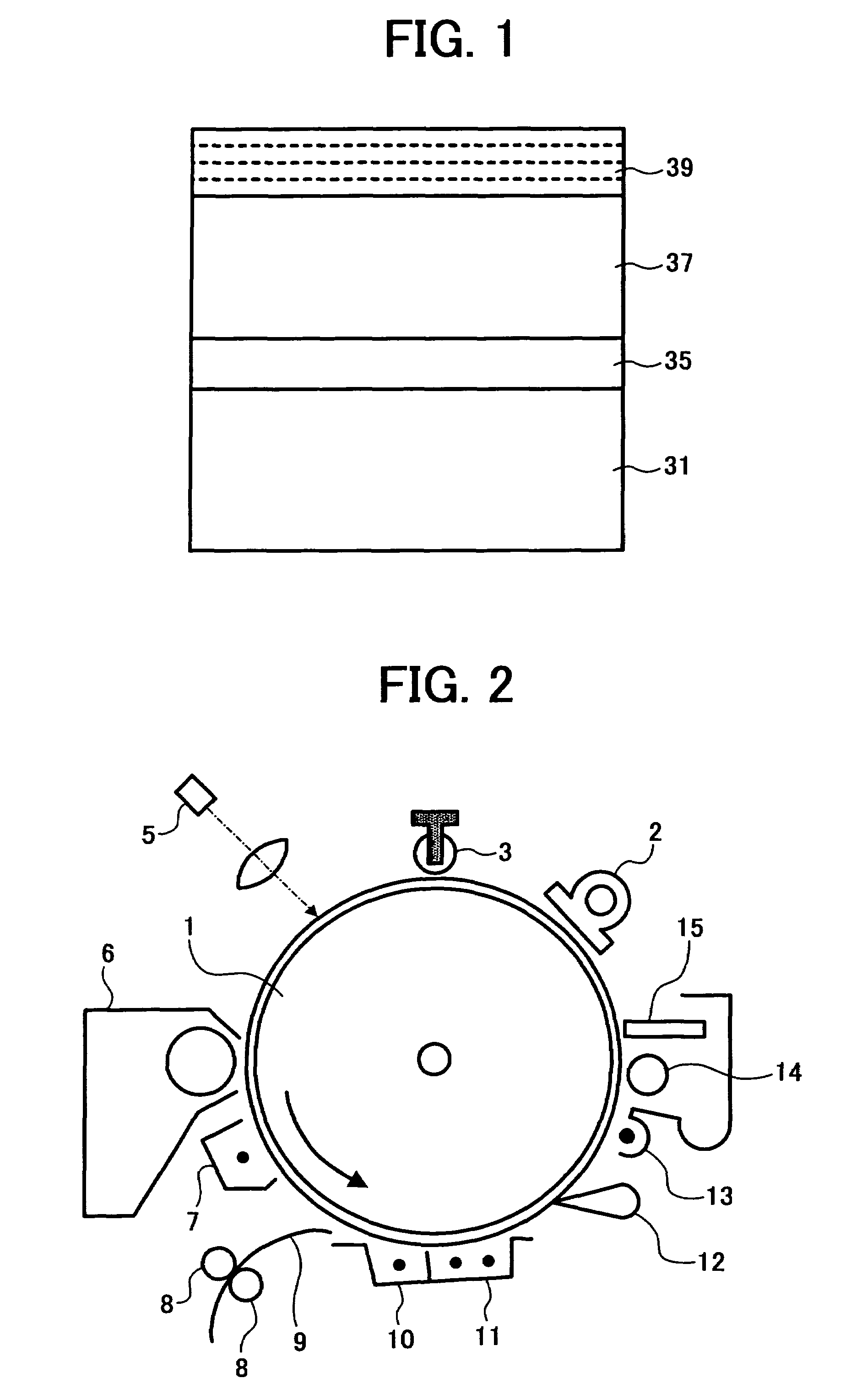
The thickness is limited to stabilize the electrostatic properties of the photoreceptor, such as charge potential and residual potential thereof in addition to the abrasion resistance and scratch resistance thereof.
However, the organic
silicon binder resin has a high hygroscopicity, resulting in deterioration of
image quality, such as blurred images due to toner filming and distorted images.
However, at the same time, abnormal images such as blurred images have noticeably been produced.
This is because a charged product becomes difficult to remove as the abrasion resistance of the photoreceptor improves.
In addition, as the abrasion resistance is improved, scratches on the surface of the photoreceptor are difficult to remove and the charged products accumulated therein are more difficult to remove.
Therefore, the surface of the photoreceptor occasionally changes in quality due to
ionization and
bond breaking because of the stress.
Although this may not cause blurred images, but the resistivity locally lowers, resulting in expansion of a dot and deterioration of image density
gradation.
It is not clear whether a
moisture accelerates such reactions or is a medium of lowering the resistivity, however, the phenomena noticeably occurs in an environment of high-temperature and
humidity.
Corona chargers are simple, but generate much
ozone and
NOx, adversely affects the electrostatic and
image properties of the photoreceptor as well as the environment.
In addition, the
corona chargers are disadvantageous for downsizing the apparatus.
However, contacting the photoreceptor, the charging member thereof is contaminated with a toner and foreign particles adhering thereto, resulting in deterioration of the chargeability of the photoreceptor; the photoreceptor is contaminated with the toner and foreign particles adhering a
gain thereto; the abrasion or uneven abrasion of the photoreceptor is accelerated with the contaminated charging member; the foreign particles removability deteriorates because the charging member is pressed against the surface of the photoreceptor; and abnormal images are produced due to a trace of the charging roller on the photoreceptor or a deformation thereof.
In addition, the charging member in this method is not easily contaminated and easy to remove the foreign particles even when adhered thereto, and therefore the charging member and the photoreceptor have higher durability.
However, the charging member and the photoreceptor need to precisely be located each other, and the charge stability of the photoreceptor tend to rather deteriorate.
An AC
voltage overlapped with a
DC voltage is applied to the charging member to improve the charge stability, which increases the charged products, resulting in production of blurred images.
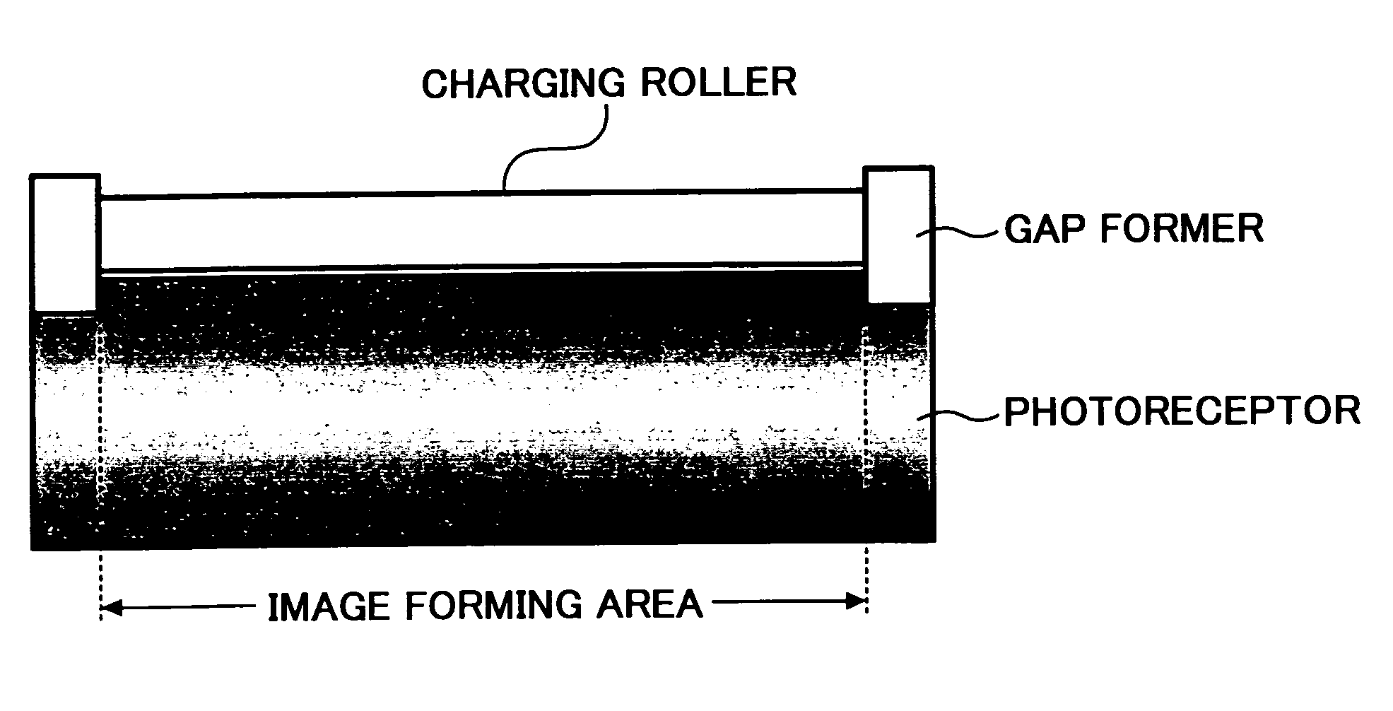
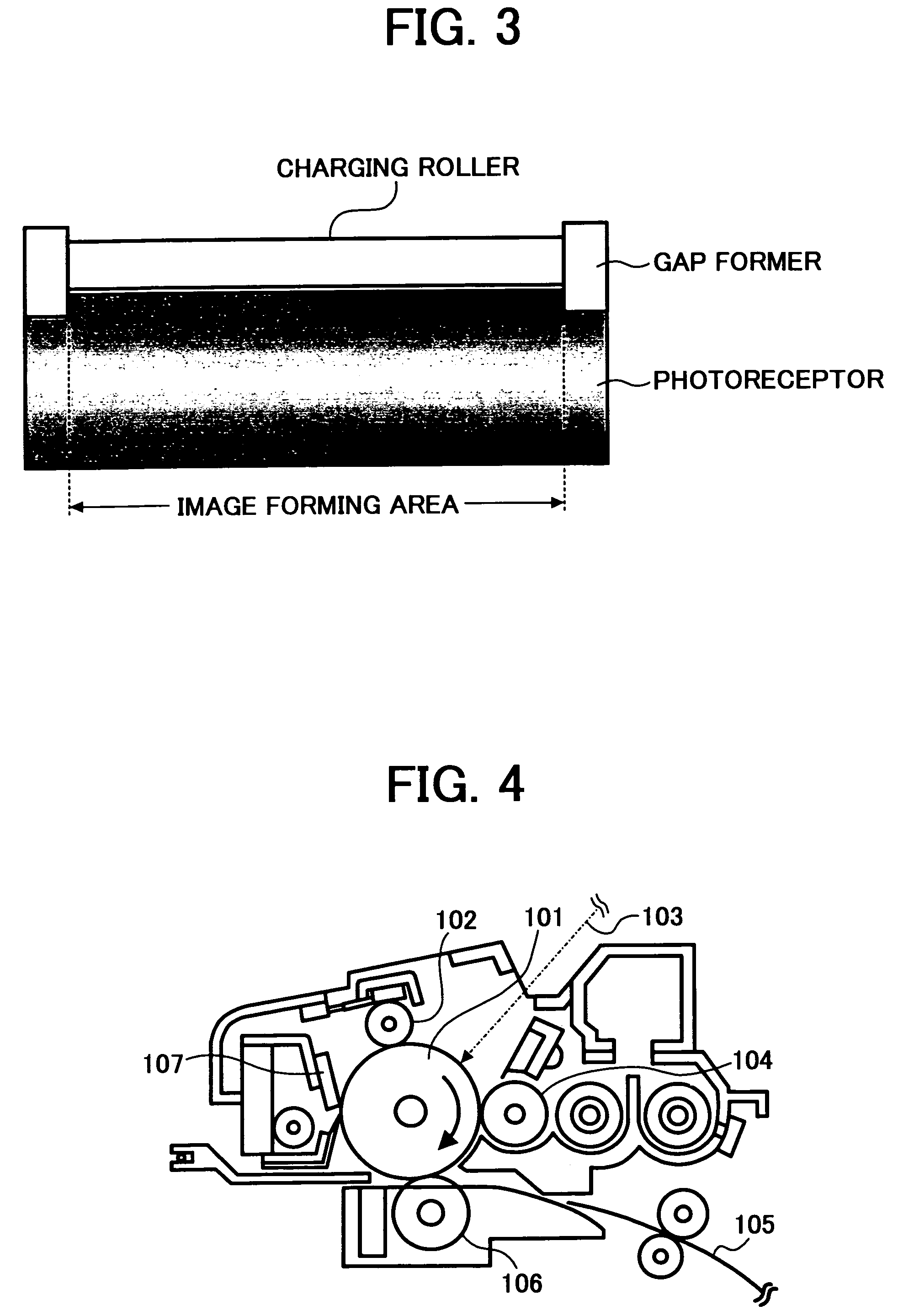
Further, a charging member located close to a conventional photoreceptor wherein a specific outermost layer is not formed on a photosensitive layer, more causes
discharge breakdown of the surface of the photoreceptor.
Therefore, even when a charging member is located close to a photoreceptor, the photoreceptor does not have higher durability as expected.
The charging member located close to a photo
receptor seems to be effectively used, however, as mentioned above, the blurred images and the
discharge breakdown of the photoreceptor rather increase, and is not effective for producing high-quality images.

