Dynamic surface annealing of implanted dopants with low temperature HDPCVD process for depositing a high extinction coefficient optical absorber layer

a technology of optical absorber layer and low temperature hdpcvd, which is applied in the direction of vacuum evaporation coating, chemical vapor deposition coating, coating, etc., can solve the problems of difficult if not impossible to achieve uniform anneal temperature across the wafer surface, deposited layer is vulnerable to cracking or peeling under the high temperature of the laser anneal step, and achieves high optical extinction coefficient (0.5)

Inactive Publication Date: 2009-09-15
APPLIED MATERIALS INC
View PDF5 Cites 3 Cited by
  • Summary
  • Abstract
  • Description
  • Claims
  • Application Information

AI Technical Summary

Problems solved by technology

The problem is that the underlying thin film structures formed on the wafer surface present different optical absorption characteristics and different optical emissivities in different locations on the wafer surface.
This makes it difficult if not impossible to attain uniform anneal temperatures across the wafer surface.
The problem of withstanding stress arises from the thermal expansion of the narrow laser-illuminated portion of the wafer surface.
One problem is that the deposited layer is vulnerable to cracking or peeling under the high temperatures of the laser anneal step, unless the layer is deposited at a very high temperature (e.g., 550 degrees C.).
Unfortunately, such a high temperature causes clustering of the implanted dopant atoms during the deposition step itself.
This results in unacceptably high sheet resistance in the source or drain regions.
This improvement is limited because the thermal annealing causes a small amount of dopant clustering which the subsequent laser annealing step cannot undo.
This results in extremely high dopant activation levels and low sheet resistance in the implanted areas, as required for 45 nm device structures.
The requirement to maintain the wafer temperature below the dopant clustering threshold temperature is critical in the 45 nm process (unlike the 65 nm process) because none of the implanted dopant atoms have been moved into substitutional crystal sites prior to laser annealing (since the thermal annealing step is not permitted), so that any elevation of the wafer temperature prior to laser annealing (e.g., during the amorphous carbon layer deposition) threatens to cluster all of the dopant atoms, which would make it impossible to obtain sufficient dopant activation even by laser annealing.
Attempting to avoid this problem by reducing the wafer temperature (e.g., below 475 degrees C.) during PECVD deposition of the absorber layer creates two problems.
First, the mechanical properties of the deposited amorphous carbon layer formed at this lower temperature are inferior so that it will fail (by cracking, peeling or separation from the wafer) during the laser annealing step.
Secondly, the amorphous carbon layer deposited at the lower temperature has inferior or insufficient optical absorption qualities (low extinction coefficient) at the 810 nm wavelength of the laser anneal step.
The extinction coefficient may be so low that the amorphous carbon layer is transparent to the 810 nm laser light regardless of thickness, and therefore is not functional.
Such a process has not seemed possible.

Method used


Image

  • Dynamic surface annealing of implanted dopants with low temperature HDPCVD process for depositing a high extinction coefficient optical absorber layer
  • Dynamic surface annealing of implanted dopants with low temperature HDPCVD process for depositing a high extinction coefficient optical absorber layer
  • Dynamic surface annealing of implanted dopants with low temperature HDPCVD process for depositing a high extinction coefficient optical absorber layer

Examples


working example

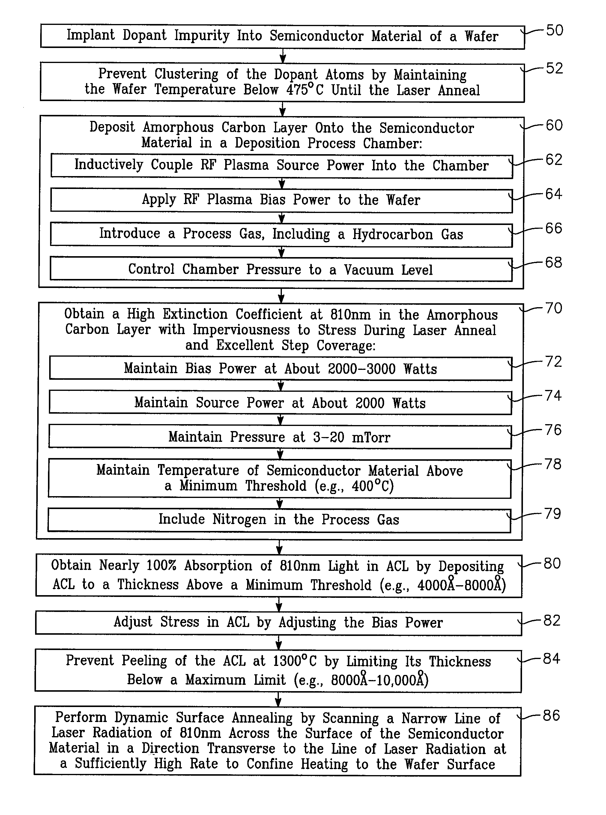
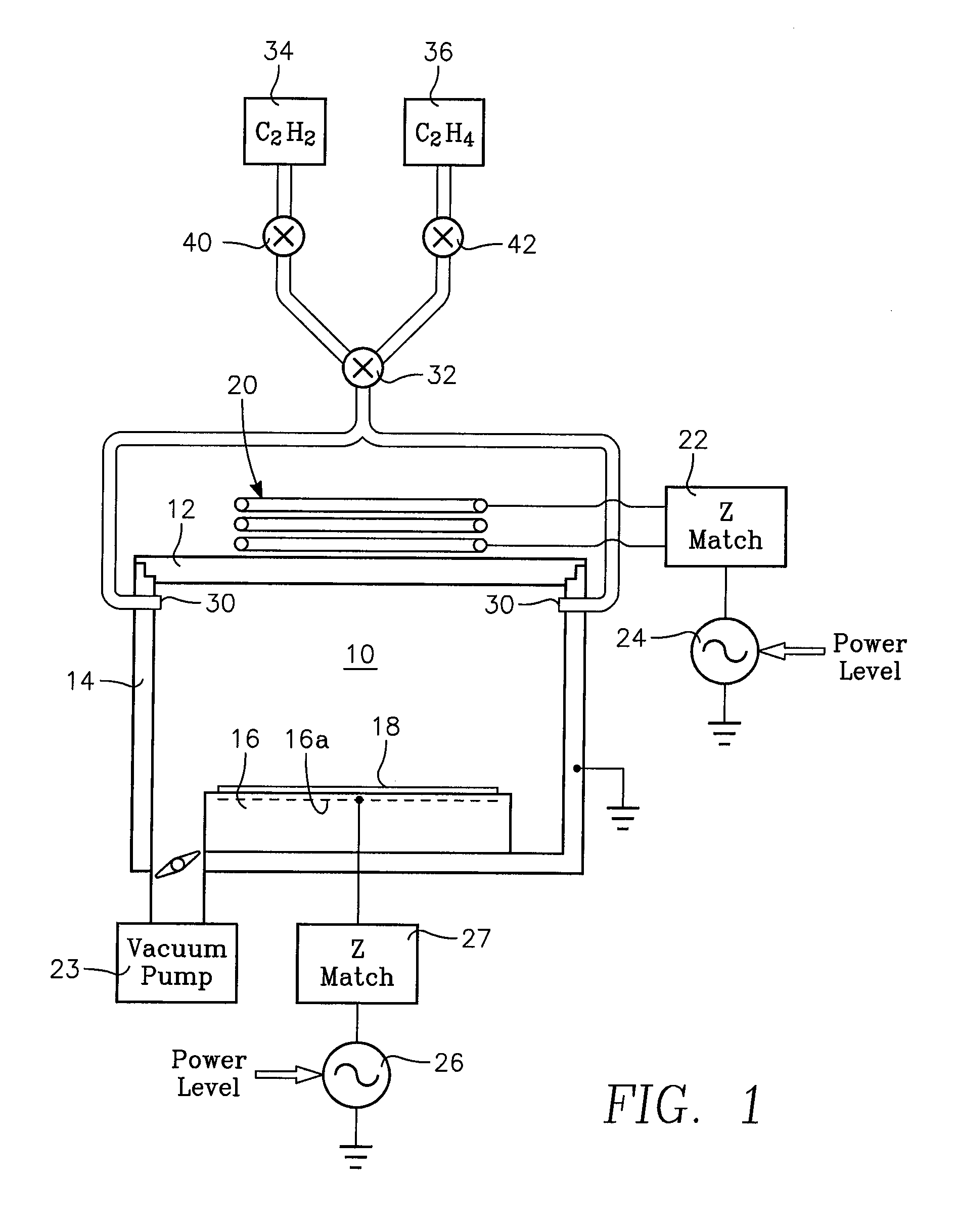
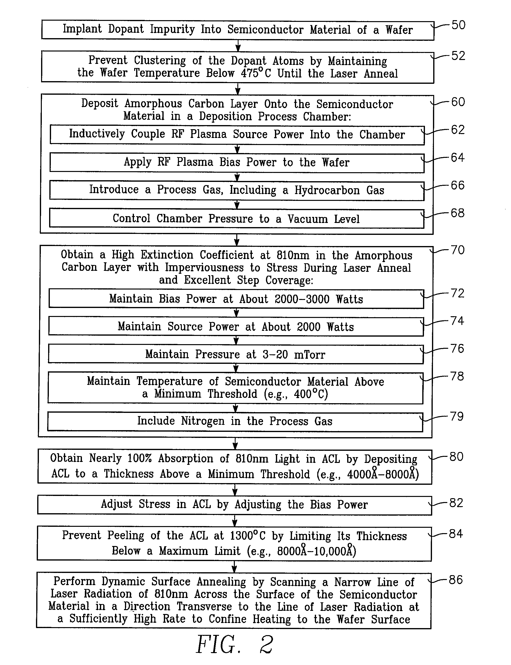
[0033]The following is a working example of the high density plasma chemical vapor deposition (HDPCVD) process of block 60 of FIG. 2. In this example, no nitrogen was present in the process gas, the process gas consisting primarily of acetylene. The process parameters were set as follows: RF plasma source power: 2,000 Watts at 2 MHz, chamber pressure: 3 mTorr, RF bias power: 2000 Watts at 13.56 MHz, process gas: Acetylene, wafer temperature: 400 degrees C. The characteristics of the ACL deposited in this example were as follows: extinction coefficient at 810 nm wavelength: 0.55, thickness: 4000 Angstroms, deposition rate: 2550 Angstroms / minute, step coverage: 100%, sidewall thickness to top thickness ratio: 100%, bottom thickness to top thickness ratio: 100%, deviation across wafer: less than 5%, damage at 1300 degrees C. during laser annealing: none.

[0034]The extinction coefficient at 810 nm obtained in the working example is 50% greater than that obtained in the high temperature P...


PUM

PropertyMeasurementUnit
pressureaaaaaaaaaa
laser wavelengthaaaaaaaaaa
bias poweraaaaaaaaaa

Abstract

A plasma enhanced physical vapor deposition process deposits an amorphous carbon layer on an ion-implanted wafer for use in dynamic surface annealing of the wafer with an intense line beam of a laser wavelength. The deposition process is carried out at a wafer temperature below the dopant clustering threshold temperature, and includes introducing the wafer into a chamber and furnishing a hydrocarbon process gas into the chamber, preferably propylene (C3H6) or toluene (C7H8) or acetylene (C2H2) or a mixture of acetylene and methane (C2H4). The process further includes inductively coupling RF plasma source power into the chamber while and applying RF plasma bias power to the wafer. The wafer bias voltage is set to a level at which the amorphous carbon layer that is deposited has a desired stress (compressive or tensile). We have discovered that at a wafer temperature less than or equal to 475 degrees C., total RF plasma source power of 4000 Watts at about 2 MHz, RF plasma bias power of 2000-3000 Watts at about 13.56 MHz and a chamber pressure in a range of 3 mTorr to 2 Torr, the deposited amorphous carbon layer has a surprising combination of high absorption and high strength and excellent step coverage.

Description

CROSS-REFERENCE TO RELATED APPLICATIONS[0001]This application claims the benefit of U.S. Provisional Application Ser. No. 60 / 841,851, filed Aug. 31, 2006.BACKGROUND OF THE INVENTION[0002]High speed integrated circuits formed on a crystalline semiconductor wafer have ultra shallow semiconductor junctions formed by ion implanting dopant impurities into source and drain regions. The implanted dopant impurities are activated by a high temperature anneal step which causes a large proportion of the implanted atoms to become substitutional in the crystalline semiconductor lattice. Such a post-ion implantation anneal step is performed using a dynamic laser surface anneal process in which a thin line of intense radiation is scanned in a direction transverse to the line across the wafer surface. The scanning rate of the line beam is sufficiently great so that heating of the wafer (to a temperature between 1150 to 1350 degrees C.) is limited to an extremely shallow depth below the surface and ...

Claims


Application Information

Patent Timeline
Patent Type & Authority Patents(United States)
IPC IPC(8): H01L21/336
CPCC23C14/5813C23C16/26H01L21/268C23C16/56H01L21/26513H01L21/26566H01L21/2658
Inventor PARIHAR, VIJAYBENCHER, CHRISTOPHER DENNISKANURI, RAJESHMENEZES, MARLON E.
Owner APPLIED MATERIALS INC
Why Eureka
Try Eureka