Methods for coating and filling high aspect ratio recessed features

a technology of recessed features and coatings, applied in the direction of coatings, metallic material coating processes, chemical vapor deposition coatings, etc., can solve the problems of reducing device dimensions, significant challenges in filling or coating such high aspect ratio nanometer and micron size structures using conventional deposition methods, and reducing device dimensions, so as to improve conformal or superconform surface coverage and improve filling in recessed features

Active Publication Date: 2009-09-22
THE BOARD OF TRUSTEES OF THE UNIV OF ILLINOIS
View PDF8 Cites 14 Cited by
  • Summary
  • Abstract
  • Description
  • Claims
  • Application Information

AI Technical Summary

Benefits of technology

[0018]The present invention provides methods for conformally or superconformally coating and / or uniformly filling structures with a continuous, conformal layer or superconformal layer. Methods of the present invention improve conformal or superconformal coverage of surfaces and improve fill in recessed features compared to conventional physical deposition and chemical deposition methods, thereby minimizing formation of voids or gaps in a deposited conformal or superconformal layer. The present methods are capable of coating or filling features useful for the fabrication of many types of electrical and electromechanical devices, including trenches, vias and relief features having physical dimensions ranging from, but not limited to, a few nanometers to 1000s of microns, and are particularly well suited for depositing a conformal or superconformal layer on and / or in high aspect ratio recessed features (e.g. aspect ratio >5). Methods of the present invention are also particularly useful for conformally or superconformally coating and / or uniformly filling reentrant features, such as recessed features having a narrowing at their openings. The present methods are compatible with a wide range of existing materials processing techniques and processing conditions, and are useful for making a wide range of functional devices including, but not limited to, integrated electric circuits, macroelectronic device arrays, memory devices, sensors, MEMS & NEMS systems, photovoltaic devices, and micro-and nanofluidic systems.
[0019]In one aspect, the present invention provides a method for depositing a conformal or superconformal layer on a recessed feature of a substrate, wherein the deposited layer conformally or superconformally coats surfaces of the recessed feature and / or uniformly fills the recessed feature. In one embodiment of this aspect of the present invention, a substrate having a recessed feature is provided, wherein the recessed feature comprises an opening, a bottom surface and side surfaces extending from the opening to the bottom surface. The recessed feature is contacted with a flow of a suppressor gas capable of accommodation on the surfaces of the recessed feature in a manner establishing a substantially steady state, anisotropic spatial distribution of the flux suppressor gas to the recessed feature. The recessed surface is also contacted with a flow of a deposition gas capable of deposition onto surfaces of the recessed feature, and optionally this step is carried out concurrently with the step of contacting the recessed feature with the flow of suppressor gas. Accommodation of suppressor gas generates suppressor on surfaces of the recessed feature that decreases the rates of deposition from the deposition gas onto surfaces having suppressor present.
[0020]In this aspect of the present invention, the flux of suppressor gas to the recessed feature generates suppressor on selected, localized regions of the surfaces of the recessed feature where suppression of the rate of deposition from the deposition gas is desired. In an aspect of the present invention useful for providing superconformal or bottom-up filling of recessed features, for example, the composition and flow rate of suppressor gas is selected such that the rate of deposition onto regions of the recessed feature proximate to (e.g. within about the upper one-third of the feature undergoing processing) the opening and / or in line-of-sight of a source of deposition gas is reduced. In this embodiment, deposition preferentially occurs on the side surfaces of the recessed feature proximate to the bottom (e.g. below about the upper one-third of the feature undergoing processing), thereby providing preferential deposition and growth of a conformal or superconformal layer onto the lower regions of the recessed layer. Use of a suppressor gas in the present invention, therefore, provides a means of controlling local deposition as a function of position in the recessed feature. In an embodiment useful for conformally or superconformally coating and uniformly filling high aspect ratio recessed features, for example, an anisotropic spatial distribution of the suppressor gas is selected to provide superconformal or bottom-up filling or coating, preferentially a substantially steady state anisotropic spatial distribution for some processing applications. Methods of this aspect of the present invention provide an inverted differential growth rate of the conformal or superconformal layer as compared to conventional CVD techniques.

Problems solved by technology

As device dimensions are reduced, however, significant challenges arise in filling or coating such high aspect ratio nanometer and micron size structures using conventional deposition methods.
These challenges constitute a barrier to achieving the desired reduction of device dimensions (e.g. <65 nanometer) in ultra-large scale integrated circuit (ULSI) architecture and the multilevel metallization therein.
Such voids and gaps are undesirable because they affect the electrical properties of the deposited layer, such as inductance, resistivity and / or capacitance, thereby, potentially degrading overall device performance and undermining device uniformity.
Further, voids and gaps in the bulk of the deposit or between the deposit and surfaces of the recessed feature compromise the overall mechanical integrity of the processed structure.
A common problem encountered in coating or filling a recessed feature, such as a trench or via, using conventional deposition methods is that the deposition rate near the opening and the bottom of the feature is often significantly larger than the deposition rate onto the sides of the feature.
As a result of enhanced deposition to the regions of the feature near the opening, flux anisotropy of deposition gas can lead to formation of an overhang proximate to the opening that prematurely seals the opening of the feature.
Sealing (or “pinching off”) of the opening prevents further deposition, thereby leaving undesirable voids or gaps in the lower regions of the recessed feature.
This problem is further exacerbated when the high aspect ratio feature being processed has small physical dimensions, such as having a width less than abut 0.1 microns, and when the deposition material has a large sticking coefficient with respect to uptake by the surface of the recessed feature.
The shape of the high aspect ratio features may also contribute to an increased likelihood of void or gap formation during filling or coating.
Reentrant features, such as a narrowing at the opening of the feature or widening at bottom of a feature, often enhances pinch-off problems during the processing of high aspect ratio features.
While at least in part addressing the some of the problems with processing high aspect ratio features, these techniques are not universally compatible with all types of deposition materials, substrates and recessed feature geometries.
In addition, each technique presents its own set of drawbacks that limit adoption and implementation of this technology.
Due to the near-unity sticking coefficient of the arriving flux in most PVD coating applications, the ability of PVD processes to coat high aspect ratio features uniformly is severely limited.
Modified PVD processes, however, such as collimated sputtering and ionized PVD have been demonstrated to provide some limited success in coating and filling moderate aspect ratio (≦5:1) features.
Film and substrate damage from high energy ions, however, can be a severe limitation in this process.
Disadvantages of these techniques include the need for intermediate photolithographic steps to define a mask layer, and the need for mechanical polishing to remove unwanted seed layer.
The disadvantage of this technique is the slow growth rate of the deposited film.
The time limit stems from the fact that the suppressor is re-emitted from the film surface at some rate and ultimately will diffuse to the bottom of the trench, despite that fact that it has a higher sticking coefficient and lower concentration with respect to the precursor.
A significant disadvantage of the time domain techniques described in Heitzinger et al. is that coating / filling larger structures requires a longer time to build up the appropriate layer thickness; and, thus, the time-limit bottom-up growth will not work because the suppressor will reach the bottom of the via before the structure is filled.
Moreover, the time delay in these systems is very short (e.g. 54.25 s in FIG. 8 and 23.92 s in FIG. 9 of Heitzinger et al.) and it is difficult to control such a short growth time during processing.

Method used


Image

  • Methods for coating and filling high aspect ratio recessed features
  • Methods for coating and filling high aspect ratio recessed features
  • Methods for coating and filling high aspect ratio recessed features

Examples


example 1

Improved Coverage and Bottom-Up Filling of Recessed Features by CVD

1.a Introduction

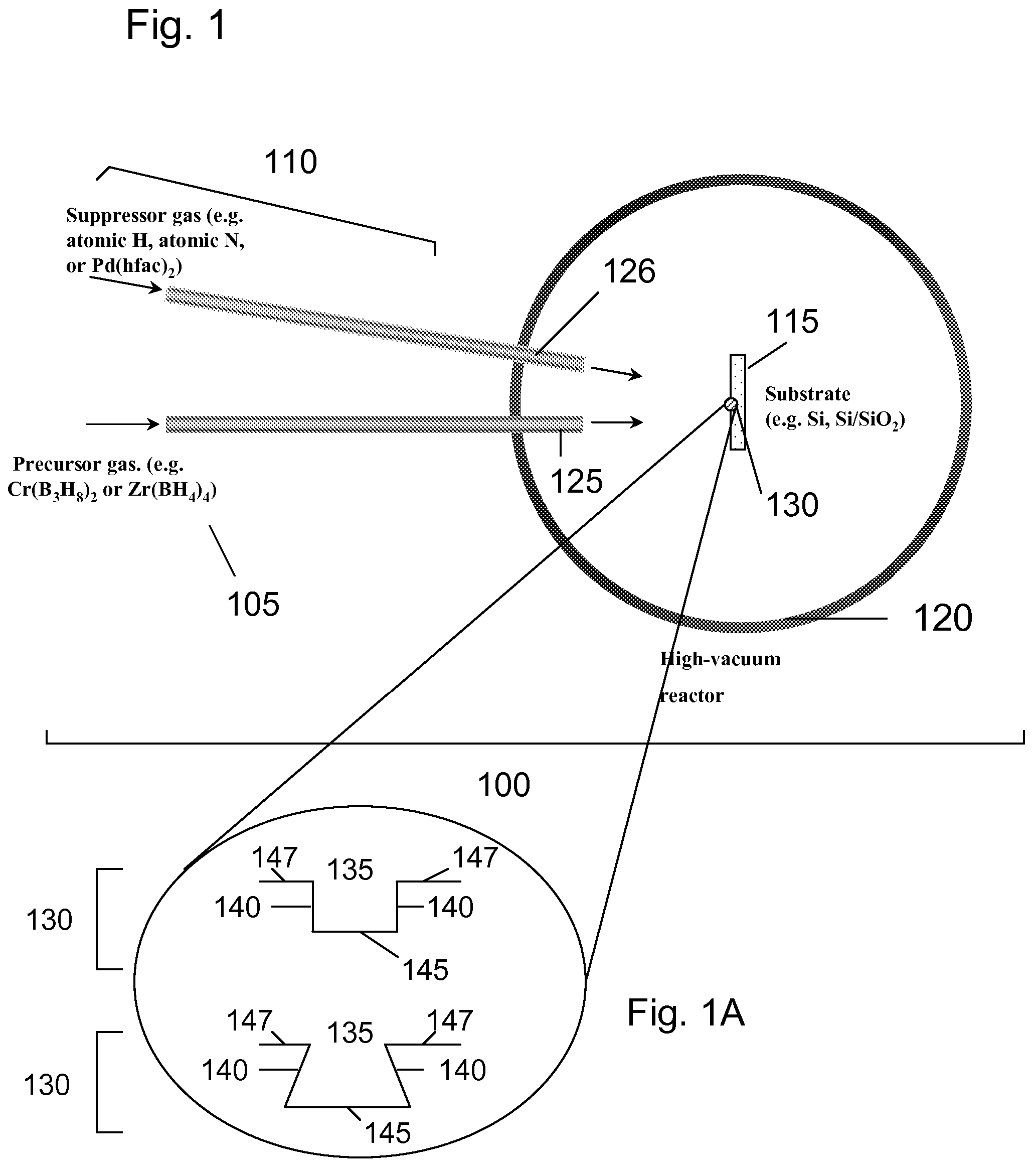
[0094]A significant challenge associated with shrinking device dimensions in ULSI architecture (≦65 nm), and the multilevel copper metallization therein, is the need to conformally or superconformally coat or to fill high aspect ratio features. (In this example, the aspect ratio is defined as the depth of the feature divided by the width of its opening.) For example, typical metallization sequence includes a silicide of Ni or Co to form the first level of contact with the device. The silicide layer resides at the bottom of a via. This is followed by uniformly coating the via with adhesion (e.g. Ti) and diffusion barrier layers (e.g. TiN). Adhesion, diffusion barrier and seed layers (for Cu electroplating) are also needed on trenches that serve as interconnect lines after being filled with copper. The general problem is that the line-of-sight flux of growth species to the lower portions of the feature ...

example 2

Methods Using Molecular Suppressor Gases

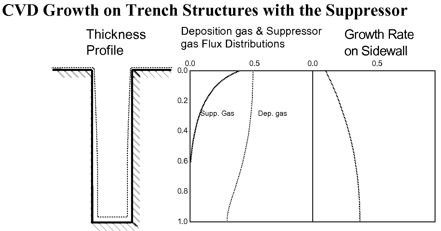
[0106]The present invention includes processing methods using molecular suppressor gases. The example provided here is the CVD growth of HfB2 films using Hf(BH4)4 as a deposition gas. The growth is strongly suppressed by bis(hexafluoroacetylacetonato)palladium, Pd(hfac)2. On planar substrates, even a small flux of Pd(hfac)2 can significantly suppress HfB2 growth. In FIG. 12, the thickness of a HfB2 film grown on a silicon substrate was measured in real-time by spectroscopic ellipsometry. The precursor pressure was kept at 0.2 mTorr throughout the process. In the first 2.5 minutes, when Pd(hfac)2 was not present, the film thickness increased linearly with time, indicating a steady state growth. However, the growth stopped immediately after the Pd(hfac)2 flow (P≦10−6 Torr) was turned on, and did not resume until shortly after the Pd(hfac)2 flow was cut off.

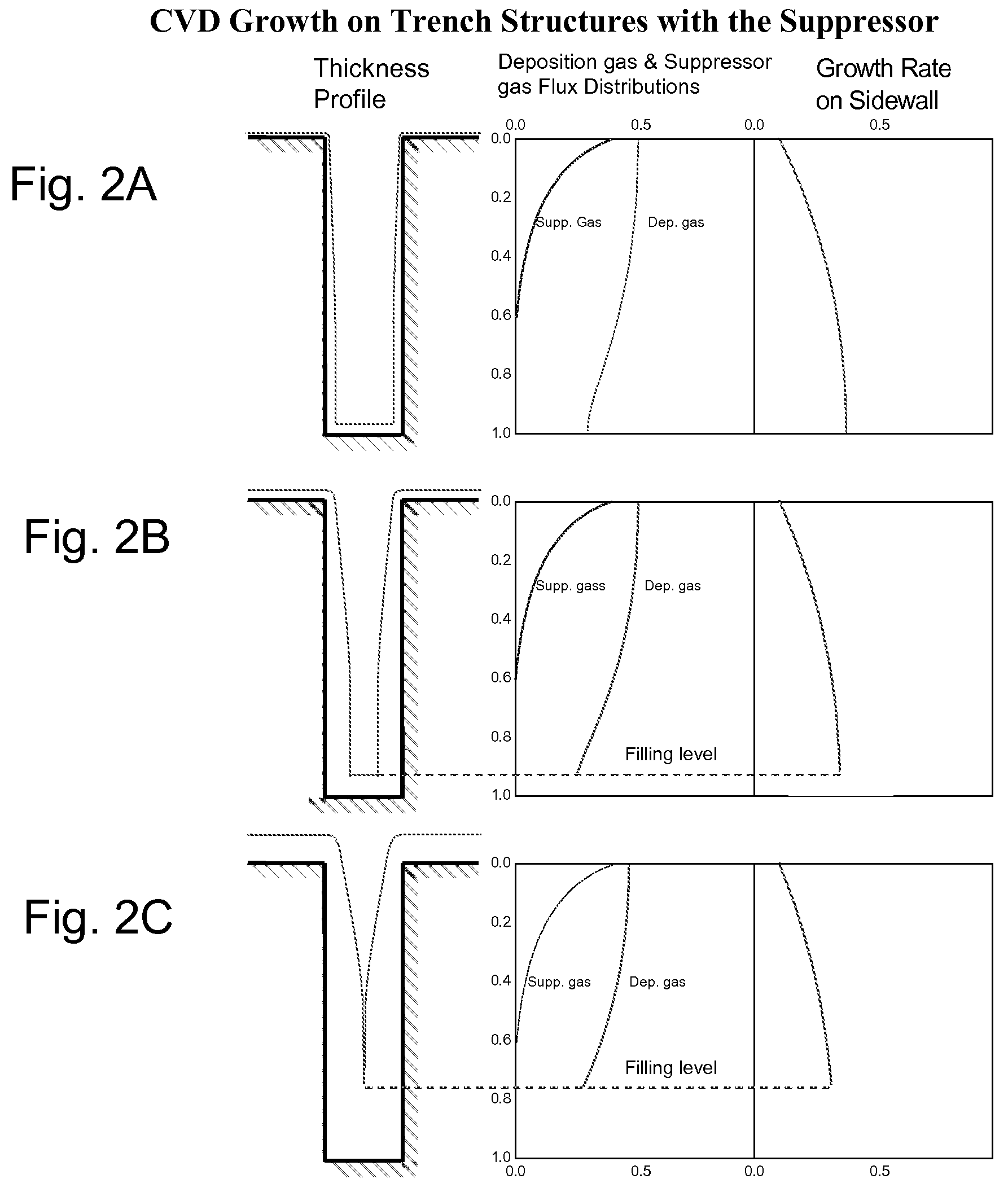
[0107]FIGS. 11A and 11B show thickness profiles of HfB2 films on the sidewall of a trench ...

example 3

Application of the Present Methods for Infiltration Deposition

[0110]Another important application of the present methods is to fill in a porous or fibrous substrate, including the interconnected pores (interstities) in a geometrically defined object such as the packing of spheres or tubes, with the material(s) supplied by a precursor or a plurality of precursors, such as one or more deposition gases. This process is commonly referred to as infiltration deposition, chemical vapor infiltration, or similar. In these applications, the present methods are used to conformally or superconformally coat recessed features and or relief features in porous or fibrous substrates. FIG. 13 provides images of a mass of carbon nanotubes infiltrated with HfB2. FIG. 14 provides a micrograph showing a coated array of packed silica spheres (colloidal crystal) generated by infiltration CVD without using a suppressor gas.

[0111]In conventional infiltration deposition techniques, a substantial challenge ari...


PUM

PropertyMeasurementUnit
aspect ratioaaaaaaaaaa
widthaaaaaaaaaa
aspect ratiosaaaaaaaaaa

Abstract

The present invention provides methods for conformally or superconformally coating and / or uniformly filling structures with a continuous, conformal layer or superconformal layer. Methods of the present invention improve conformal or superconformal coverage of surfaces and improve fill in recessed features compared to conventional physical deposition and chemical deposition methods, thereby minimizing formation of voids or gaps in a deposited conformal or superconformal layer. The present methods are capable of coating or filling features useful for the fabrication of a broad class of electronic, electrical and electromechanical devices.

Description

CROSS REFERENCE TO RELATED APPLICATIONS[0001]This application claims priority under 35 U.S.C. 119(e) to U.S. provisional Patent Application 60 / 732,007 filed Nov. 1, 2005, which is hereby incorporated by reference in its entirety.STATEMENT REGARDING FEDERALLY SPONSORED RESEARCH OR DEVELOPMENT[0002]This invention was made, at least in part, with United States governmental support awarded by National Science Foundation Grants NSF CH 0076061, NSF DMR 0315428 and NSF DMR 0420768. The United States Government has certain rights in this invention.BACKGROUND OF INVENTION[0003]Substrate patterning techniques combining advanced lithographic processing and material deposition methods enable the fabrication of structures on substrate surfaces having well defined physical dimensions ranging from 10s of nanometers to 1000s of microns. These material processing methods are compatible with a wide range of substrate and deposition materials, including many dielectric, semiconducting and conducting m...

Claims


Application Information

Patent Timeline
Patent Type & Authority Patents(United States)
IPC IPC(8): H01L21/44
CPCH01L21/314C23C16/045H01L21/02107
Inventor ABELSON, JOHN R.JAYARAMAN, SREENIVASGIROLAMI, GREGORY S.YANG, YUKIM, DO YOUNG
Owner THE BOARD OF TRUSTEES OF THE UNIV OF ILLINOIS
Why Eureka
Try Eureka