Mobile, transportable, electrostatic chuck for wafers made of semiconductor material

a technology of electrostatic chucks and semiconductor materials, which is applied in the direction of electrostatic charges, capacitors, weapons, etc., can solve the problems of long time-consuming, inconvenient transportation, and inability to conduct diodes reverse biased, so as to reduce the likeliness of diodes, avoid the effect of conductivity and high breakdown voltag

Inactive Publication Date: 2010-01-26
RETZLAFF UDO HEINZ
View PDF24 Cites 7 Cited by
  • Summary
  • Abstract
  • Description
  • Claims
  • Application Information

AI Technical Summary

Benefits of technology

[0008]In view of the shortcomings described above, the object of the invention is to create mobile, transportable electrostatic chucks (Mobile Chucks) at a reasonable cost with low leakage currents and high Young's Modulus values, which show a good insulation of the electrodes against unintentional discharging effects due to open contact areas, which are accessible to the outside environment with humidity and liquids and which keep a high, long lasting clamping force and a stable shape under those conditions without being connected with a power supply unit.
[0012]Also according to the invention an additional dielectric layer can be build up on to of the open contact area. This additional dielectric layer has typically a high ∈r-value, for example made of lead-barium-strontium-titanate or yttrium oxide. There break-down voltage is designed in a way that the electric breakdown occurs below the charging voltage, what enables the charging. This means that the breakdown voltage of the additional dielectric layer is less than the breakdown voltage of the dielectric layer of the Mobile Chuck itself. After the first charging process a microscopic small breakdown channel of a few micrometer or manometers is created. This breakdown channel is much smaller than the about one millimeter diameter contact holes. During the following charging processes this existing microscopic breakdown channel is used again. Even small deviations of the contact needles can be compensated, because surface current effects will guide the current flow again to the week insulation point. Thus only a microscopic small contact point is created. This microscopic small contact point is hardly to be wetted. This is of advantage for the insulation of the contact area against liquids. It is known that different cleaning procedures are available in the semiconductor technology which can build up hydrophobic surfaces on a dielectric layer. This reduces the likeliness of wetting the channels and thus avoids there conductivity. Microscopic small channels also can be produced with alternative procedures like laser drilling. Also a damp-proofing membrane made of PTFE (Poly-Tetra-Fluoro-Ethylene) can be added to avoid the penetration of liquids. Procedures to manufacture those layers are known from the textile industry. Those membranes are big enough to enable damp to pass through but no liquids. During the unintentional discharging those above described extra layers reduce or even eliminate together or instead of the introduced pn-junction the early, complete discharging of Mobile Chucks.

Problems solved by technology

This results in a long time lasting, sufficient high electrostatic clamping force.
Diodes which are reverse biased cannot conduct.

Method used


Image

  • Mobile, transportable, electrostatic chuck for wafers made of semiconductor material
  • Mobile, transportable, electrostatic chuck for wafers made of semiconductor material
  • Mobile, transportable, electrostatic chuck for wafers made of semiconductor material

Examples


first embodiment

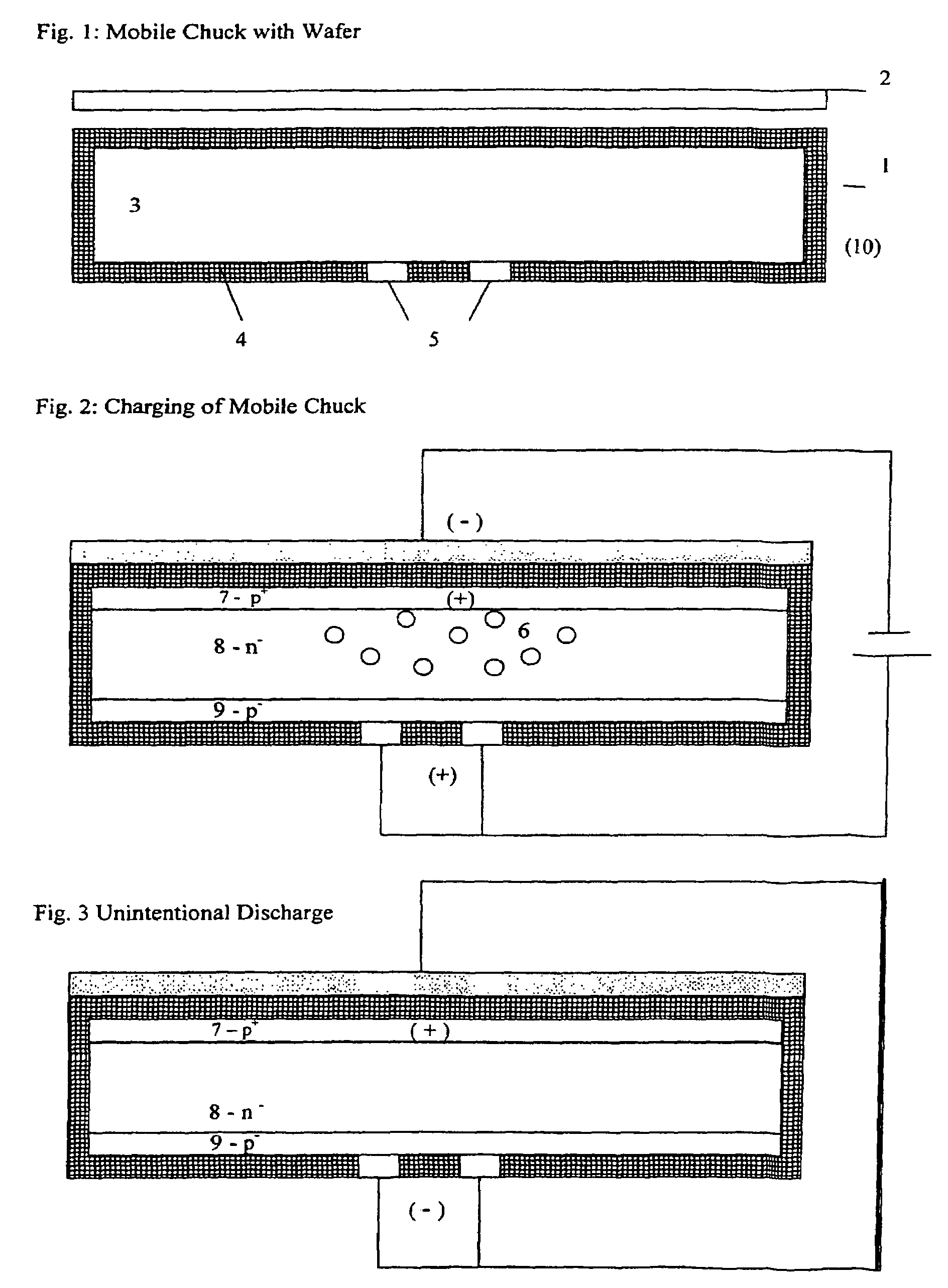
[0022]The first embodiment describes a capacitor structure of a unipolar Mobile Chuck (1) with clamped wafer (2), as shown in FIG. 1. The Mobile Chuck (1) is build up from a double side polished silicon wafer as semiconductor material (3), a 3.5 μm thick dielectric layer (4) from silicon dioxide and 100 nm silicon nitride with the opened contact holes (5) on the backside. The contact holes (5) are reaching through to the semiconductor material (3) and are used to contact the Mobile Chuck (1) during charging and discharging. The wafer (2) to be clamped, works as the first electrode and the semiconductor—material (3) acts as the second electrode of the capacitor structure. Both electrodes are separated electrically with the dielectric insulating layer (4).

embodiment 350

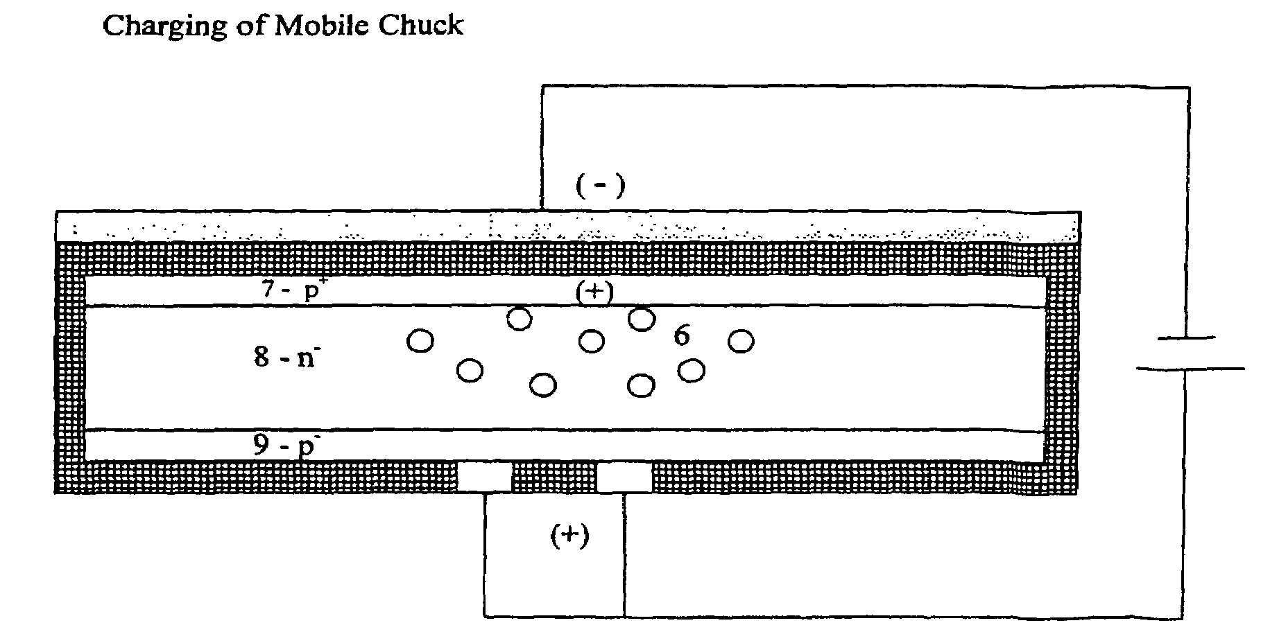
[0023]The application of a clamping voltage of 300 V, as described in FIG. 2, generates an electric field between the negative charged—or grounded—wafer (2) and the positive charged semiconductor material (3). The wafer (2) attracts the Mobile Chuck (1) and is now electro-statically clamped (activated). In accordance with the invention, within the substrate material (3) there are differently doped (p- and n-type) semiconductor layers (7,8,9) arranged. The substrate material (3) is a silicon wafer itself, phosphorus doped, n-type with a specific resistance of 10-20 Ohm*cm. This n−-type bulk region (8) has the lowest doping level. That's why the depletion region is extending deep into the low doped bulk region. The break trough voltage of the pn-junction is designed to avoid Punch-Through-effects, avalanche breakdown and to reach low leakage currents, herby the breakdown voltage of the diode should be about double than the charging voltage. The thickness of the bulk region (8) is in t...

second embodiment

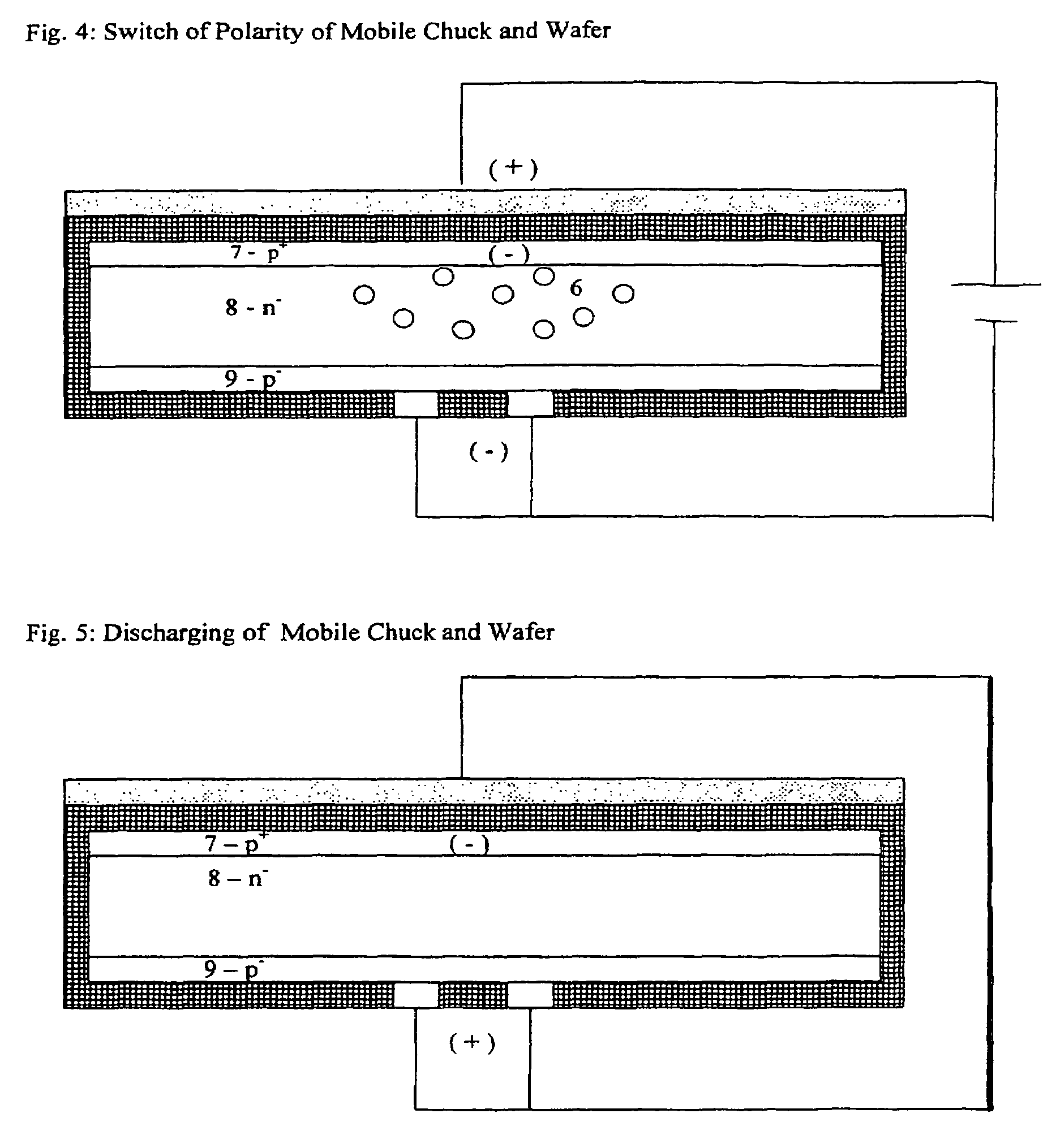
[0025]The second embodiment describes a Mobile Chuck (1) according to FIG. 6 with differently doped (p- and n-type) semiconductor layers (8,9), where the area (9) is only locally brought in into the substrate material (3). The p−-type doped area (9) shows only a local limited extension into the n−-type bulk region (8). The advantage is that the pn-junction has only a relatively small geometrical extension. This smaller size results in a smaller capacity of the depletion region and thus reduces the switching time of the diode (pn-junction of region 8 and 9) as well as the reverse current. The dielectric layer (4) has a thickness of about 2 μm, which enables the doping of the area (9) after the contact holes (5) are open. Implantation of e.g. Boron through the open contact holes (5) directly into the bulk material and followed by a drive in diffusion creates a locally limited p−-type doped area (9). The 2 μm thick dielectric layer (4) is used as implantation mask for the area (9) and ...


PUM


Abstract

A mobile, transportable, unipolar electrostatic chuck for clamping thin wafers is described, which avoids unintentional discharging of the package of Mobile Chuck and wafer during wet processing. Short circuits between the contact holes of the chuck and the clamped wafer can lead to the loss of clamping force. A pn-junction within the semiconductor substrate material electrode of the chuck is disclosed, which is using a diode effect to avoid the loss of charges. Dielectric protection layers of PTFE, Y2O3 or ferroelectric materials can be used to cover the open contacts of the chuck. This enables the application of Mobile Chucks also for wet etch-, photo- and cleaning processes. Mobile Chucks are made of semiconductor material and semiconductor manufacturing processes are applied. Those Mobile Chucks have nearly identical properties as the clamping substrate itself. This reduces the risk of cross-contamination, particle generation and the risk of mechanical stress due to different coefficients of thermal expansion.

Description

FIELD OF THE INVENTION[0001]The present invention relates to an electrostatic chuck made of semiconductor material for wafer handling and especially to mobile, transportable electrostatic chucks, were the Mobile Chuck keeps clamping a thin wafer after charging (applying a clamping voltage) without permanent connection to an external power supply unit for transportation or other process steps up to several hours. As used herein, a “wafer” encompasses any of the various types of substrates that can be held on a chuck, including semiconductor wafers, solar cells, glass or ceramic plates, or any of various other suitable substrates.BACKGROUND OF THE INVENTION[0002]Wafers are used in the Semiconductor and Solar industry. Typically they are round or have a stable, rectangular shape. Semiconductor wafers of 4″ up to 12″ are used with a standard thickness between 500 μm up to 875 μm. But there active elements, e.g. transistors have a pn-junctions depth of only 0, 1 to 5 μm. Thus, most of th...

Claims


Application Information

Patent Timeline
Patent Type & Authority Patents(United States)
IPC IPC(8): H01T23/00H01L21/683F41B15/04H01G7/02H05F3/00
CPCH01L21/6831H01L21/6833
Inventor RETZLAFF, UDO HEINZ
Owner RETZLAFF UDO HEINZ
Why Eureka
Try Eureka