Charged-particle exposure apparatus

a particle exposure and charge technology, applied in the field of particlebeam projection processing apparatus, can solve the problems of affecting local charging effects, pd system sensitive, and components of electron-optical systems that are likely to be contaminated by these particles, so as to avoid severe contamination and related risks, improve particle purity, and avoid the effect of severe contamination

Active Publication Date: 2010-06-15
IMS NANOFABTION
View PDF8 Cites 11 Cited by
  • Summary
  • Abstract
  • Description
  • Claims
  • Application Information

AI Technical Summary

Benefits of technology

[0008]It is a goal of the present invention to provide a particle-beam system using an additional foil, in the following referred to as “transmission foil”, in the region of the beam after the PD system in which overcomes the above-mentioned problems. The provision of a foil is meant to separate spaces containing different gases and / or gas pressures. This enables the use of a mechanical scanning system, which can be run at a residual pressure significantly higher than those that are usually acceptable within an electro-optical device, so existing air bearing stages operated typically at 1-10 mbar can be used. It further allows of a significant improvement of particle purity at the optical columns and APS, and offers a means to avoid a severe contamination and related risks when used in a semiconductor fabrication line.
[0009]This aim is met by a particle-beam projection processing apparatus of the kind as described above, which further comprises at least one transmission foil located across the path of the patterned beam, said foil(s) being positioned between the pattern definition means and the position of the target at a location close to a respective image of the aperture pattern formed by the projection system. The transmission foil may be made of an electrically conductive material and is held at a well defined electrical potential, so the charged particle beam is neither affected by local charging at the surface or inside the foil, nor by a floating electrical field due to a floating foil potential. It shall be mentioned that the transmission foil may be made as well of an insulating or semiconducting material provided above-mentioned effects (charging, floating potential) are compensated directly or indirectly by either the transmitting beam itself (e.g. by creating electron-hole pairs, etc.), or other supplementary measures which improve charge transport or charge balance along the foil, such as in-situ irradiation with UV light or atomic beams.
[0012]The implementation of such a foil is possible since in the type of apparatus considered here, the beam has a wide cross-section. In other systems such as a TEM or a Gaussian beam writer, the imaging optics provide for a beam focused to a narrow, almost point-like, image location. The latter would destroy or contaminate a foil within a comparably short time, not only because of the exposition to radiation, but also due to heating imparting by absorption. In contrast, with the invention the beam is distributed over a comparatively wide area which allows sufficient cooling of the foil, which is done by thermal radiation and conductive cooling over the edge of the foil. Calculations made be the applicants showed that a foil of 0.2 μm will heat up by about 170 K only during continuous exposure to an electron beam in a PML2 apparatus even if only conductive cooling is taken into account. The current density on the foil in the present invention is about 10−07 A / cm2 (assuming here 10 μA current through a 1 mm2 area), which is about 10 million times lower than that in a typical focused beam system.
[0015]In order to deal with beam components which are scattered off by angles that are too high to be processed in the electron-optical system, an aperture diaphragm may be located after the transmission foil as seen along the direction of the beam, said diaphragm having an aperture limiting the lateral extension of the beam. This measure also rules out problems that may occur with regard to higher-order imaging coefficients.
[0017]Beside the possibility to use the foil as a plate electrode, the foil is a barrier for gas particles, thus separating the electrooptical column into different sections which may have different vacuum properties (gas filling, pressure) and preventing contamination between sections thus formed. Only fast particles, namely the particles (e.g. electrons) of the particle beam, are able to overcome this mechanical barrier. Thus, the transmission foil may separate two adjacent recipients held at different gas pressures. The transmission foil may, preferably, be continuous across the area of the respective image of the aperture pattern, in order to ensure uniform transparency behavior for each part of the image. The thickness is then chosen suitably (minimum thickness) to allow passage through the foil only for particles having a minimum kinetic energy.

Problems solved by technology

Also components of the electron-optical systems (e.g. lenses and APS) are likely to be contaminated by these particles or, what is unavoidable in lithographical use, by organical resist outgassing from the wafer.
The particles may be accelerated into the column, whereas mainly the PD system is sensitive to contamination and, as a consequence, might be affected by local charging effects.
However, the required high vacuum stage is a major technical issue and cost factor of an overall lithography system like the PML2.
Additionally, an important concern for the use of an PML2 apparatus in the semiconductor fabrication environment is connected with the danger of system failure, which could be due to a break down of parts of the aperture plates or electron source.
Such an event could lead to severe contamination of the wafer, wafer stage and wafer handling systems.
It is not possible, though, to achieve a lens of negative refractive power by means of annular electrodes alone; on the contrary, it is necessary to use a plate or control grid electrode through which the beam passes.
However, it is often desirable to have a diverging lens located after the mask or PD device, without involving the latter (particularly if its electrostatic potential cannot be controlled to a satisfactory degree).
For such a diverging lens located after the mask or PD device, the plate electrode will cause unwanted effects, most notably absorption and scattering of the beam radiation.
For modern structuring purposes, where the minimum feature size is more and more pushed towards lower values, scattering is the most disturbing effect since it leads to blurring of the pattern features.

Method used


Image

  • Charged-particle exposure apparatus
  • Charged-particle exposure apparatus
  • Charged-particle exposure apparatus

Examples


example 1

Foil Near to the Final Image

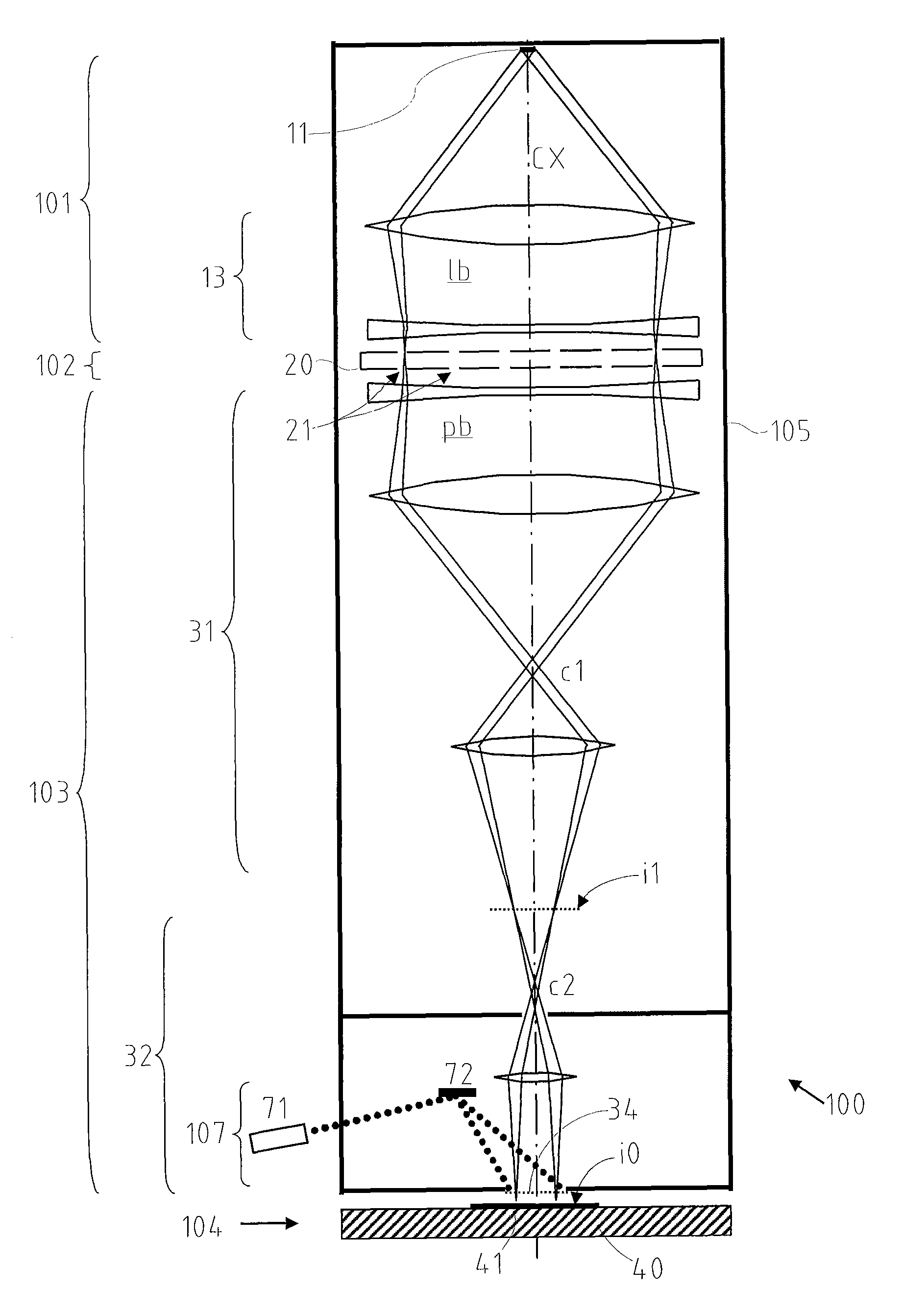
[0040]In the first embodiment which is shown in FIG. 1, a thin transmission foil 34 is placed between the last lens and the substrate, so as to bring the foil near to the position of the final image. Preferably, the distance between the foil 34 and the target 41 is very small, in the range of 200-500 μm. While elastic and / or inelastic scattering of some part of the electrons in the foil is inevitable, which will rise to an additional contribution to the blur of imaging (scattering blur), by virtue of the small distance between the foil and the substrate the scattering blur contribution is very small. Details of scattering are further discussed below. The inelastically scattered electrons have a reduced kinetic energy, but at the end of the column the field of the lenses is zero and therefore the trajectory of the electrons is not changed (there is not extra chromatic blur).

[0041]For a gap between the foil and substrate of Δl=200 μm, the allowed extra blur...

example 2

Foil at the Intermediate Image

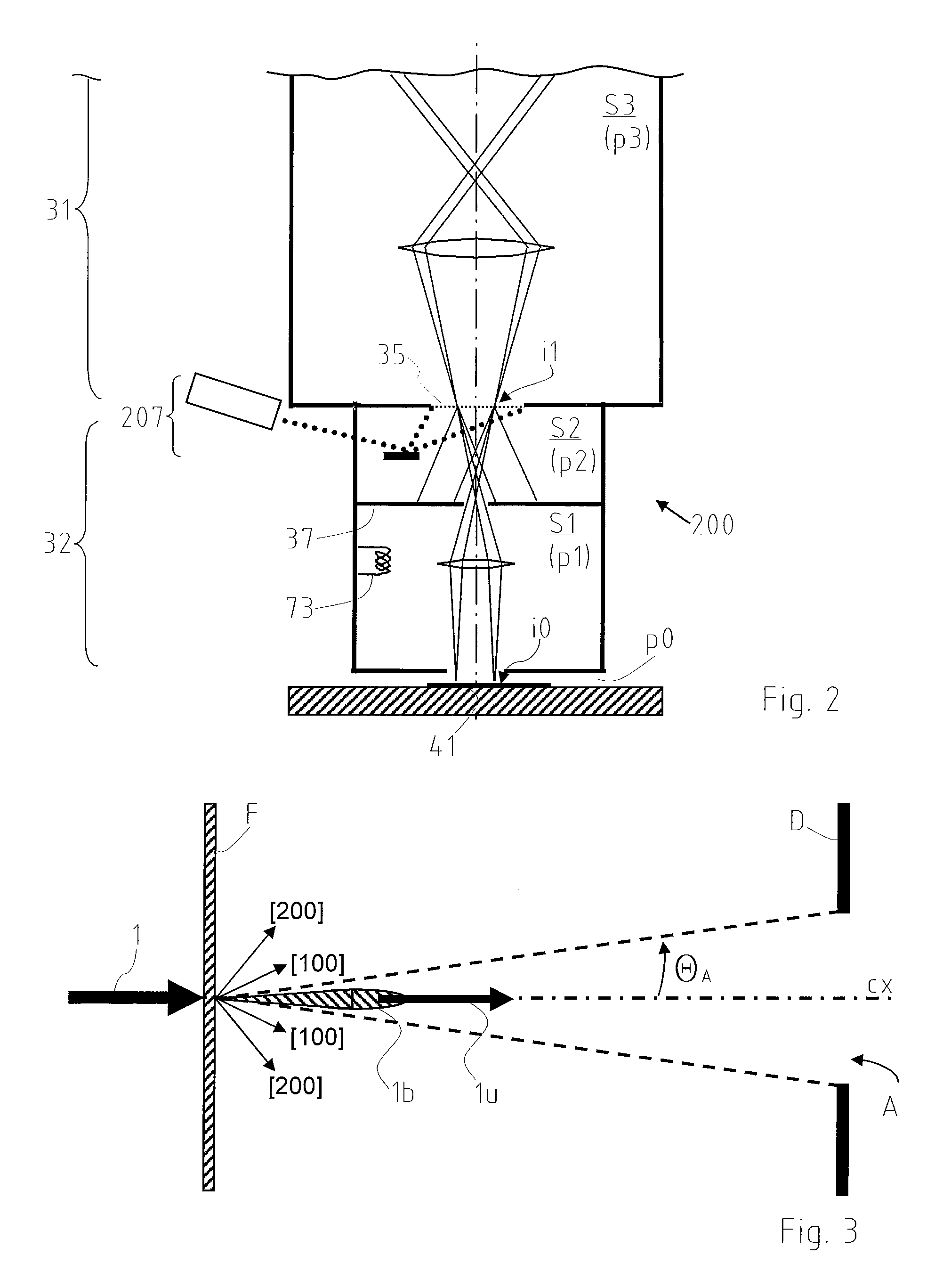
[0046]FIG. 2 illustrates a second embodiment 200 of the invention, in which a part of the apparatus 200 is shown; elements of the apparatus 200 not described below are identical to those of the apparatus 100 of FIG. 1; same reference numbers refer to corresponding elements throughout.

[0047]As a consequence of the fact that the foil 35 is located at the position of the intermediate image i1, electrons which are scattered off their initial beam path are, nonetheless, focused at the final image plane i0 to the zero loss peak. Electrons which are scattered with a higher angle than 1.1 mrad have an increased spherical aberration, and these electrons are suitably blanked by a blanking diaphragm 37 situated after the foil 35.

[0048]The foil 35 divides the apparatus 200 into consecutive sections. In the first section S3, comprising the source 11, illuminating system 101, the PD device 102 and the part of the projection system until the intermediate image i1, is ...

example 3

Two Foils

[0065]FIG. 4 shows another embodiment of the invention, namely an apparatus 300 which comprises two foils 34′,35′ both at the intermediate image and in front of the target. Thus, the beneficial features of the foils can be combined. In particular, the foil 35′ at the intermediate image reduces the coulomb interaction at the last cross over and the total current through the coulomb can be increased (the coulomb interaction blur is the dominate blur), while the final foil 34′ prevents contamination of the optical components of the second stage 32 due to resist out gassing since the section S1 is not vacuum separated from the pressure p0 above the target 41.

Interlock Sensor and Safety Valve

[0066]As shown in FIGS. 5a and 5b, the foil may also be used as an interlock sensor to realize a safeguard device in conjunction with a safety valve. The safeguard device is used to rapidly trigger a safety valve in case of mechanical or electrical breakdown that causes a destruction of the ...


PUM


Abstract

A particle-beam projection processing apparatus for irradiating a target, with an illumination system for forming a wide-area illuminating beam of energetic electrically charged particles; a pattern definition means for positioning an aperture pattern in the path of the illuminating beam; and a projection system for projecting the beam thus patterned onto a target to be positioned after the projection system. A foil located across the path of the patterned beam is positioned between the pattern definition means and the position of the target at a location close to an image of the aperture pattern formed by the projection system.

Description

CROSS-REFERENCE TO RELATED APPLICATIONS[0001]This application is a U.S. National Stage application of PCT Application No. PCT AT06 / 000060, filed Feb. 16, 2006, which claims priority from Austrian Patent Application No. A 273 / 2005, filed on Feb. 18, 2005.FIELD OF THE INVENTION AND DESCRIPTION OF PRIOR ART[0002]The invention relates to improvements on particle-beam projection processing apparatus for irradiating a target by means of a beam of energetic electrically charged particles, comprising an illumination system, a pattern definition (PD) means and a projection system in order to project the beam patterned by the PD means onto a target positioned after the projection system. The illumination system serves to generate and form the energetic particles into a wide-area illuminating beam which is substantially tele / homocentric at the location of the PD means and whose diameter is greater by at least one order of magnitude than the length of the tele / homocentricity region of the illum...

Claims


Application Information

Patent Timeline
Patent Type & Authority Patents(United States)
IPC IPC(8): G21G5/00
CPCB82Y10/00B82Y40/00H01J37/3175H01J37/3174H01J2237/31793H01J2237/31788
Inventor PLATZGUMMER, ELMARCERNUSCA, STEFANSTENGL, GERHARD
Owner IMS NANOFABTION
Why Eureka
Try Eureka