
Porous insulating film, method for producing the same, and semiconductor device using the same

a porous insulating film and semiconductor technology, applied in the direction of semiconductor/solid-state device details, coatings, chemical vapor deposition coatings, etc., can solve the problems of deteriorating circuit operation speed, increase in wiring delay, and increase in wiring delay

Active Publication Date: 2011-06-28
RENESAS ELECTRONICS CORP
View PDF30 Cites 13 Cited by
  • Summary
  • Abstract
  • Description
  • Claims
  • Application Information

AI Technical Summary

Benefits of technology

The approach results in a stable porous insulating film with a low specific inductive capacity, improved adhesion, and reduced parasitic capacitance, enhancing the operational speed and reliability of semiconductor devices while minimizing material waste and production costs.

Problems solved by technology

This is associated with a tangible increase in wiring delay resulting from a progress in micronization of wiring width and wiring pitch.
Therefore, an increase in capacitance between wires leads to a remarkable increase in wiring delay, bringing about a deterioration in circuit operation speed resultantly.
Although the fluorine-added SiO2 can reduce specific inductive capacity when fluorine in the film is concentrated, it raises a problem that moisture absorption increases.
Further, there is another problem that hydrogen fluoride produced by a reaction between moisture and hydrogen corrodes wiring materials and a rise in specific inductive capacity due to desorption of fluorine.
However, this method has the following problem.
Therefore, the utility effect of a raw material is low and the production cost is therefore increased.
Also, when oxygen molecules are present in the air during heating, these oxygen molecules react with the monomers and there is the case where an intended film structure is not obtained.
It is therefore necessary to substitute the whole gas of the baking furnace with inert gas to remove oxygen molecules in the air during heating, which is a hindrance to cost reduction.
Moreover, a coating and heating step is carried out in each layer when multilayer wiring is formed and therefore the lowermost wiring layer repeatedly receives heat stress at high temperatures for a long time.
This is a cause of a reduction in reliability, especially, of the deterioration of fined copper wiring.
As a result, the characteristics of the porous insulating film changes with time, resulting in an unstable porous film.
However, in the above plasma CVD method, the starting raw material gas is dissociated into an atomic level in plasma and on principle, it is not that a structure reflecting the molecular skeleton of the starting material is grown.
However, it is difficult to control the process of forming a film of the activated atom in the plasma and it is difficult to control the structure of a growing porous insulating film.
Namely, it is basically difficult to control the size and filling density of pores in the film for obtaining a low dielectric constant.
Also, because this method needs large plasma power to dissociate the starting material, it gives rise to the problem that a semiconductor device receives a large damage.
Moreover, when the pore diameter is increased to about 3 nm or more, moisture, process gas, chemical solutions and the like easily enter into the insulating film and the strength of the film lowers, with the result that this causes a deterioration in the reliability of the insulating film and lower adaptability to a process of manufacturing a semiconductor device.
However, if the ratio of polar elements is decreased, the surface density of these polar elements is decreased on the interface between the film and other semiconductor materials and also the film has such a structure that its composition abruptly changes at the contact interface, with the result that it is difficult to maintain high adhesiveness.

Method used


Image

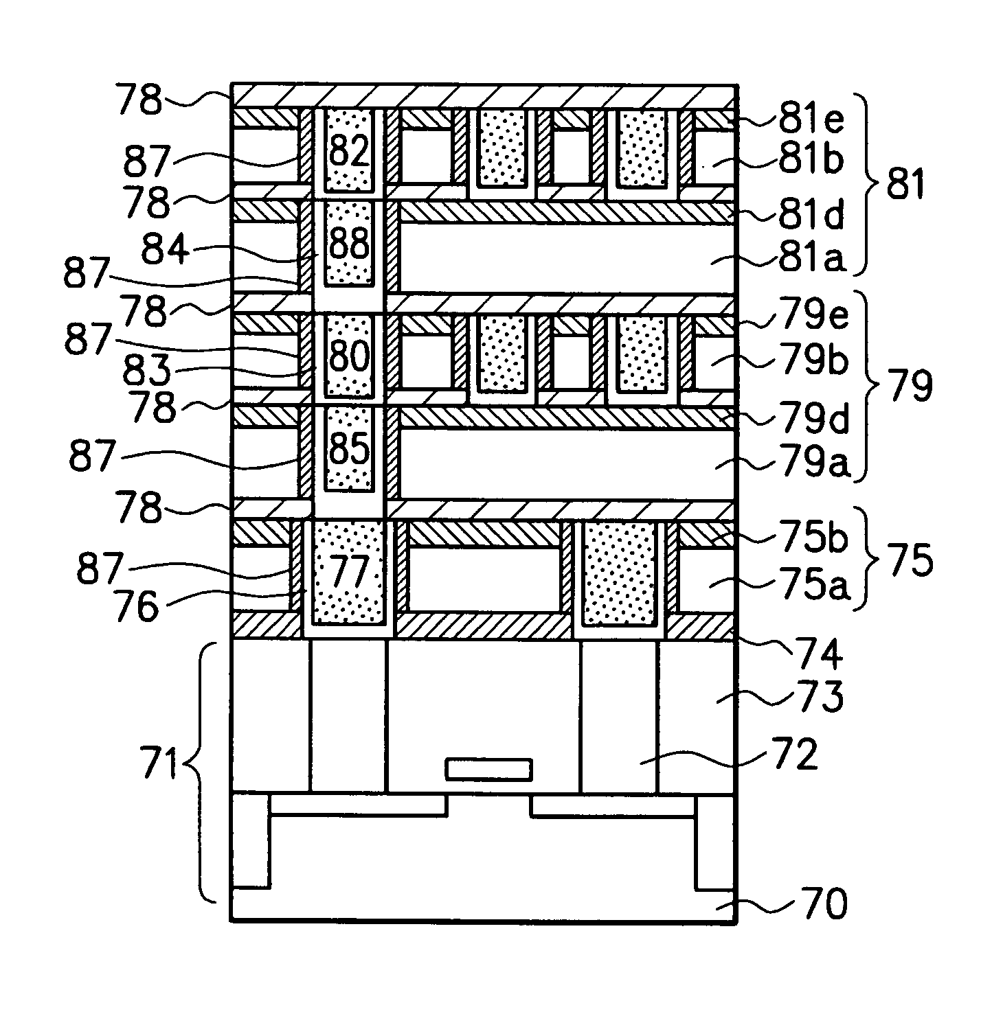
  • Porous insulating film, method for producing the same, and semiconductor device using the same
  • Porous insulating film, method for producing the same, and semiconductor device using the same
  • Porous insulating film, method for producing the same, and semiconductor device using the same

Examples


first embodiment

[0120]As a first embodiment to practice the present invention preferably, explained is an insulating film formed using, as starting material, a cyclic organic silica compound raw material which has a cyclic silica skeleton in its molecule, wherein at least one unsaturated hydrocarbon group is bound with the cyclic silica skeleton.

[0121]The insulating film according to this embodiment is formed using tetravinyl-tetramethylcyclotetrasiloxane (TVTMCTS) monomers as one of the cyclic organic silica compound raw material which has a cyclic silica skeleton and in which at least one unsaturated hydrocarbon group is bound with the cyclic silica skeleton in its molecule.

[0122]For comparison, other insulating films were also formed using two kinds of material different from that of the insulating film in this embodiment.

[0123]One of these insulating films (first comparison insulating film) was formed using tertiary butyltriethoxysilane monomers (TBTES) represented by the formula (14), which is...

second embodiment

[0159]In this embodiment, a process was carried out in which a trivinyltriisopropylcyclotrisiloxane (3V3IPC3S) monomer represented by the formula (4) was used as the raw material to grow a layer insulating film. The cyclic organic siloxane of 3V3IPC3S (n=3) contains less cyclic siloxane skeletons than the cyclic organic siloxane of TVTMCTS (formula 7) (n=4). Therefore, the diameter of an inside hole constituted of the cyclic skeleton of 3V3IPC3S is 0.35 nm φ, which is smaller than that (0.45 nm φ) of the cyclic skeleton of TVTMCTS.

[0160]Though the unsaturated hydrocarbon which is one side chain of the cyclic siloxane is common to a vinyl group, the other side chain is a methyl group in the case of TVTMCTS and an isopropyl group, which is a bulky side chain, in the case of 3V3IPC3S. Specifically, 3V3IPC3S is characterized by smaller-diameter pores in a cyclic skeleton and more bulky saturated hydrocarbon side chains and unsaturated hydrocarbon side chains.

[0161]In the gasification co...

third embodiment

[0167]As a third embodiment of the present invention, an insulating film obtained when using tetravinyltetramethylcyclotetrasiloxane monomers as starting material and nitrous oxide (N2O) as oxidizer gas will be explained.

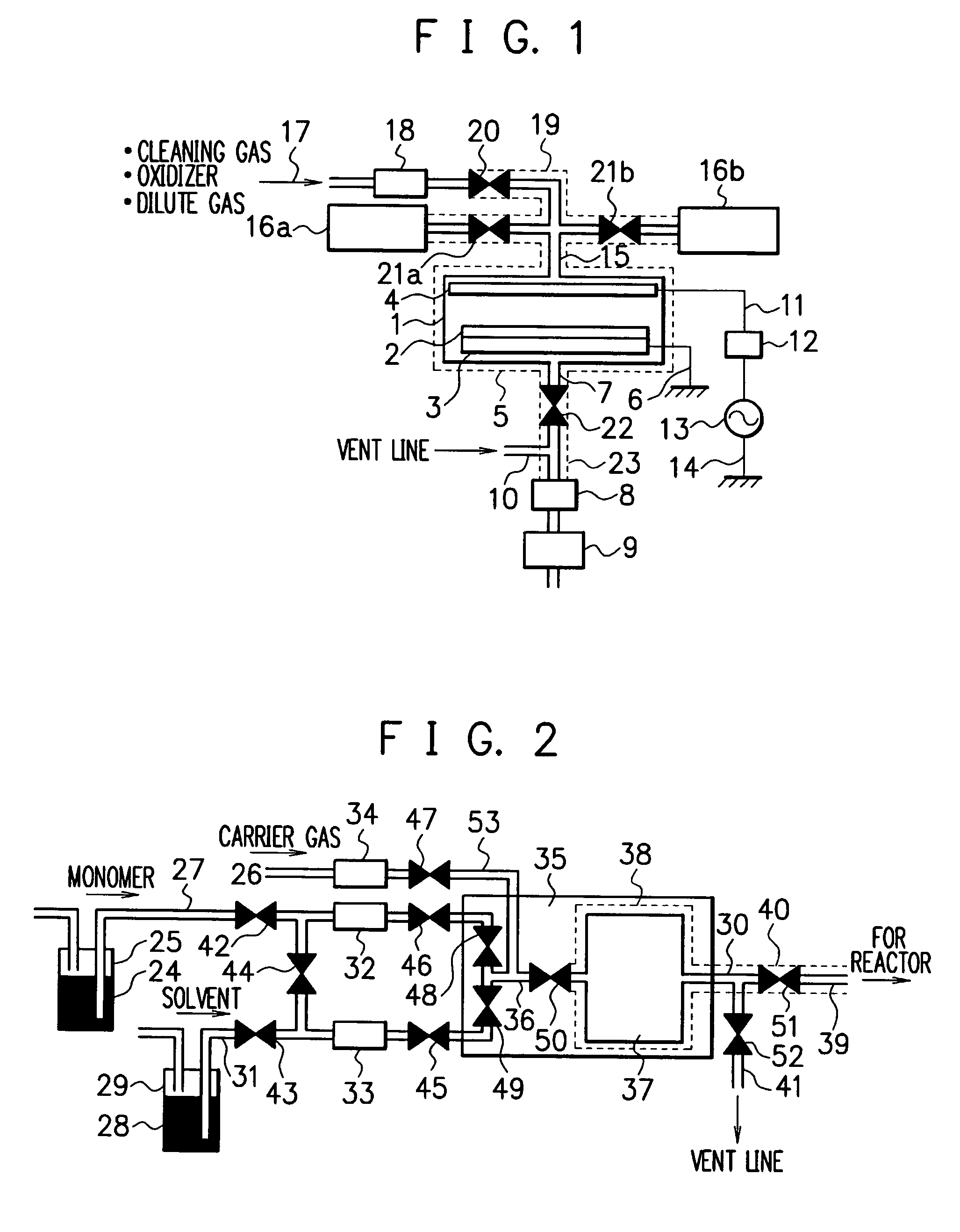
[0168]In this embodiment, 8.450×10⁻¹ Pa·m3 / s of helium was supplied as the carrier gas. The tetravinyltetramethylcyclotetrasiloxane monomers were gasified in the gasification controller 35 shown in FIG. 2 and supplied in an amount of 1.099×10⁻¹ Pa·m3 / s. Helium of 1.690×10⁻¹ Pa·m3 / s acting as diluent gas was led into the reaction chamber 1. In addition, N2O of 5.408×10⁻² Pa·m3 / s to 2.197×10⁻¹ Pa·m3 / s was led into the reaction chamber 1.

[0169]In the reaction chamber 1, the semiconductor substrate 2 was placed in advance on the substrate heating part 3 kept at 350° C. The pressure in the reaction chamber 1 was reduced to 360 Pa, and high frequency voltage (frequency: 13.56 MHz and RF power: 200 W) was applied to the shower head 4 to generate plasma, thereby growing an ...


PUM

PropertyMeasurementUnit
diameteraaaaaaaaaa
pore diameteraaaaaaaaaa
temperatureaaaaaaaaaa

Abstract

The present invention provides a process of producing a porous insulating film effective as an insulating film constituting a semiconductor device and a process of producing a porous insulating film having high adhesion to a semiconductor material, which is in contact with the upper and lower interfaces of the insulating film. Gas containing molecule vapor of at least one or more organic silica compounds, which have a cyclic silica skeleton in its molecule and have at least one or more unsaturated hydrocarbon groups bound with the cyclic silica skeleton is introduced into plasma to grow a porous insulating film on a semiconductor substrate.

Description

FIELD OF THE INVENTION[0001]The present invention relates to a porous insulating film usable as an insulating film constituting a semiconductor device, to a method of producing the porous insulating film and to a semiconductor device utilizing the porous insulating film.BACKGROUND ART[0002]Along with recent technological development, more highly integrated and higher density semiconductors have been developed. This is associated with a tangible increase in wiring delay resulting from a progress in micronization of wiring width and wiring pitch.[0003]The wiring delay is proportional to the product of wiring resistance and capacitance between wires and wiring resistance tends to be increased along with the aforementioned micronization of wiring width. Therefore, an increase in capacitance between wires leads to a remarkable increase in wiring delay, bringing about a deterioration in circuit operation speed resultantly. Therefore, in order to raise the circuit operation speed of a semi...

Claims


Application Information

Patent Timeline
Patent Type & Authority Patents(United States)
IPC IPC(8): H01L21/31C23C16/40H01L21/316
CPCC23C16/401H01L21/02126H01L21/02203H01L21/02211H01L21/02216H01L21/02274H01L21/02304H01L21/02362H01L21/31695H01L2924/0002H01L2924/00
Inventor HARADA, YOSHIMICHIHAYASHI, YOSHIHIROITOH, FUMINORIHIJIOKA, KENICHIROTAKEUCHI, TSUNEO
Owner RENESAS ELECTRONICS CORP
Learn More