Method of fabrication of cubic boron nitride conical microstructures

a technology of cubic boron nitride and conical microstructure, which is applied in the direction of polycrystalline material growth, crystal growth process, chemically reactive gas growth, etc., can solve the problems of poor cbn film properties including sensitivity to humidity, excessive stress, and delamination of films thicker than 200 nm, so as to improve the effect of chemical vapor deposition, high adhesion and extreme support capacity

Active Publication Date: 2012-04-17
CITY UNIVERSITY OF HONG KONG
View PDF2 Cites 1 Cited by
  • Summary
  • Abstract
  • Description
  • Claims
  • Application Information

AI Technical Summary

Benefits of technology

[0017]The adherent cBN films are deposited on diamond layer by either plasma enhanced chemical vapor deposition (PECVD) or physical vapor deposition (PVD) methods. Cubic BN films can be grown on diamond films directly in either a single or multi-step growth process using a wide range of particle energies from hundreds of eV down to energies close to the thermal particle energies. The diamond layer beneath the cBN film provides the structural compatibility, high adhesion, extreme supporting capacity for any mechanical applications and enables heteroepitaxial growth of cBN films. The absence of amorphous BN (aBN) / turbostratic BN (tBN) interface makes the cBND composite insensitive to humidity.

Problems solved by technology

The practical application of cBN in film forms has also been hampered because the incompatibility of cBN with many types of substrates primarily in their physical properties and the process of synthesis, which leads to the poor cBN film properties including sensitivity to humidity, excessive stress, and delamination of film thicker than 200 nm.
However, availability of suitable cBN films and then their high switch-on electric field have hampered using them in these applications.
However, Cubic BN nanostructures such as nanocones have not been possible hitherto because of the significant difficulties in preparing fundamental structures of cBN films with satisfactory quality and thickness over large areas.

Method used


Image

  • Method of fabrication of cubic boron nitride conical microstructures
  • Method of fabrication of cubic boron nitride conical microstructures
  • Method of fabrication of cubic boron nitride conical microstructures

Examples


example

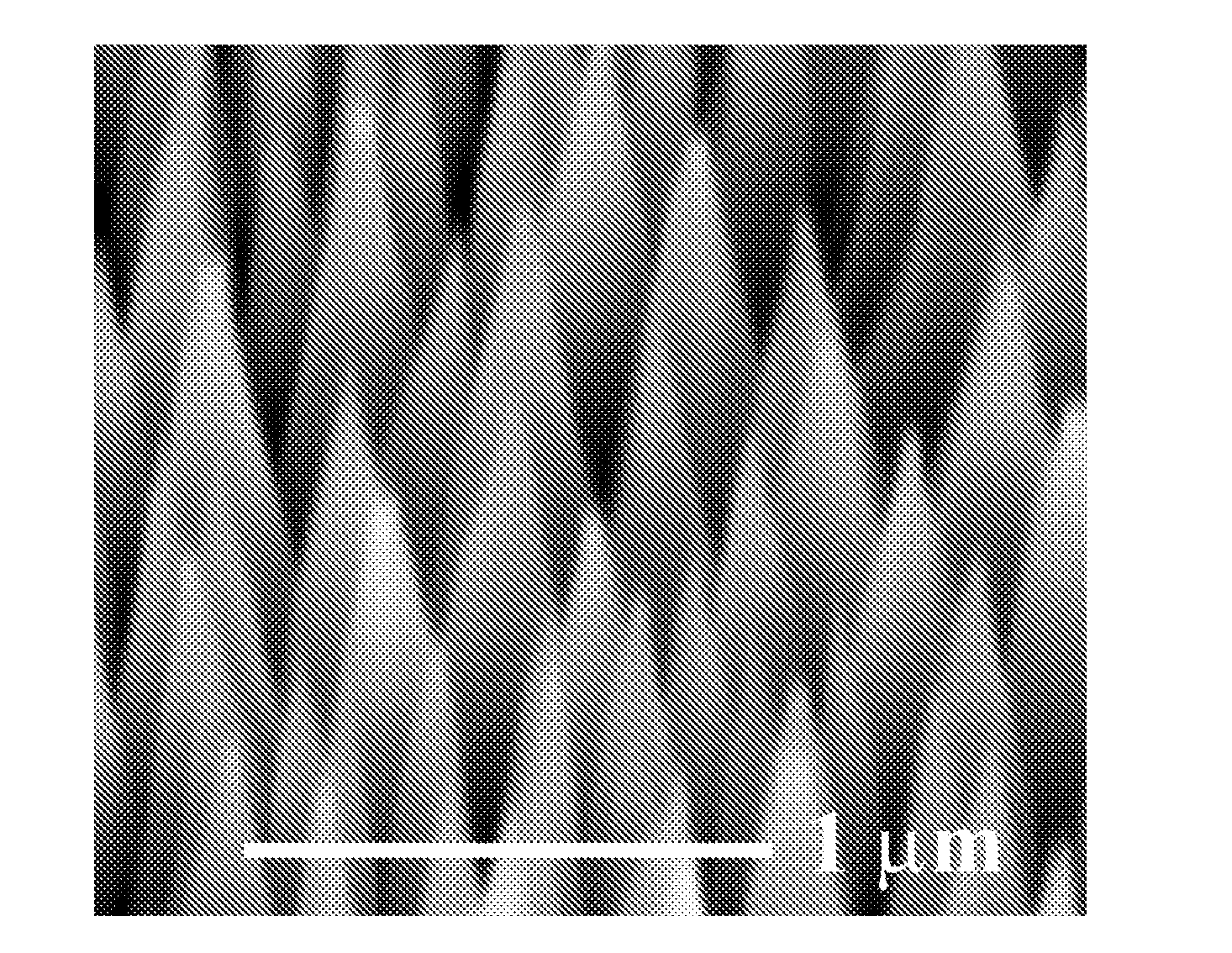
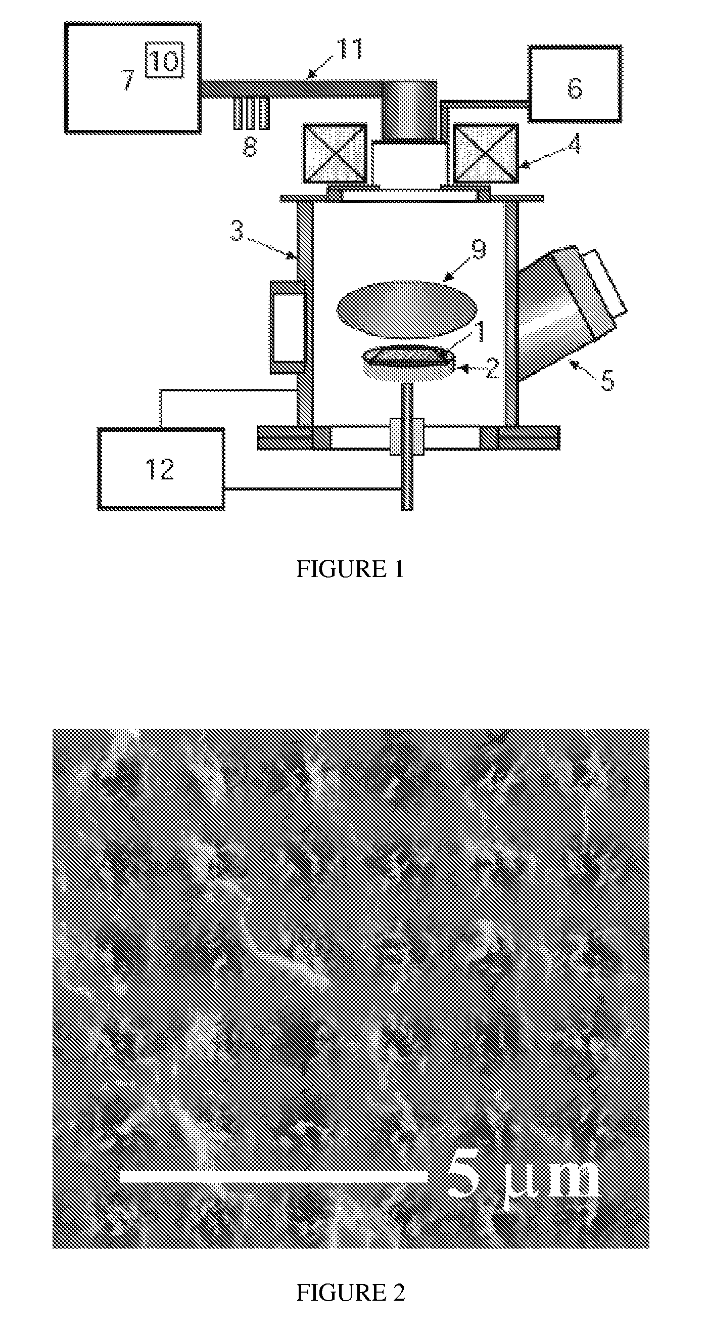
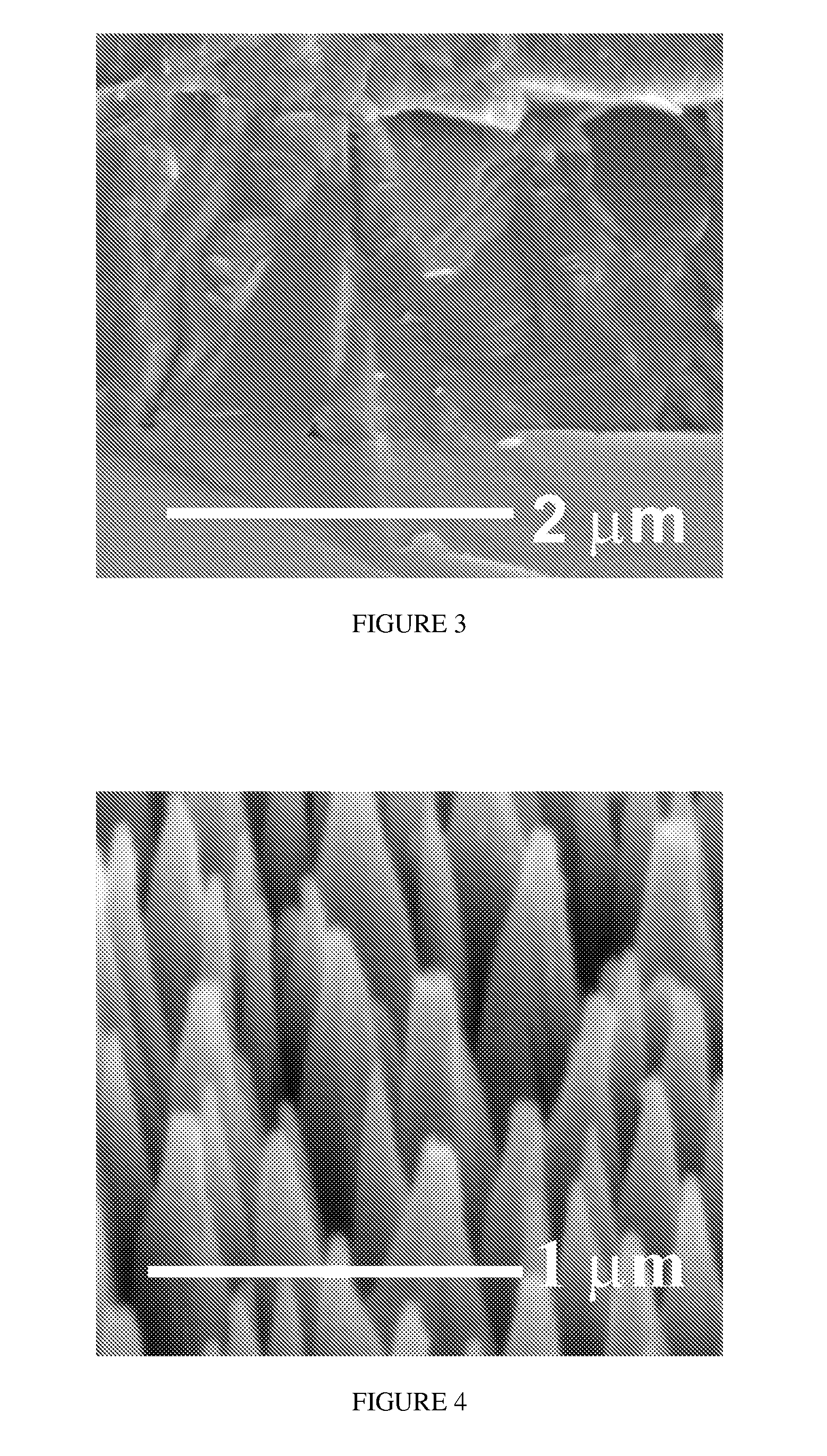
[0041]A polycrystalline diamond film was first deposited on silicon (001) substrate using the CVD apparatus shown in FIG. 1. Prior to the diamond deposition, the substrate was scratched by diamond powder with a grain size of about 100 nm to enhance the diamond nucleation. During the deposition, plasma was induced in a 0.5% CH4 / 99.5% H2 mixture at a pressure of 30 Torr and total gas flow rate of 300 sccm. The deposition temperature was maintained at 850° C., and the microwave power was 1200 W.

[0042]The cBN film was subsequently deposited in the same apparatus, BF3, N2, He, Ar, and H2 at gas flow rates of 1, 50, 140, 10 and 2 sccm, respectively, were supplied into the reaction chamber from a gas supply unit to secure the operation pressure of 2×10⁻³ Torr. Using these conditions and a magnetic field of ˜875 gauss applied to the central region of the reaction chamber employing an external magnetic coil, the deposition was carried out in an electron cyclotron resonance (ECR) mode. The mi...


PUM

PropertyMeasurementUnit
pressureaaaaaaaaaa
grain sizeaaaaaaaaaa
temperatureaaaaaaaaaa

Abstract

A conical structure of cubic Boron Nitride (cBN) is formed on a diamond layered substrate. A method of forming the cBN structure includes steps of (a) forming diamond nuclei on a substrate, (b) growing a layer of diamond film on the substrate, (c) depositing a cBN film on said diamond layer, (d) pre-depositing nanoscale etching masks on the cBN film, and (e) etching the deposited cBN film. In particular, though not exclusively, the cubic Boron Nitride structure has great potential applications in probe analytical and testing techniques including scanning probe microscopy (SPM) and nanoindentation, nanomechanics and nanomachining in progressing microelectromechanical system (MEMS) and nanoelectyromechanical system (NEMS) devices, field electron emission, vacuum microelectronic devices, sensors and different electrode systems including those used in electrochemistry.

Description

BACKGROUND OF THE INVENTION[0001]1. Field of the Invention[0002]The current invention relates to conical microstructures of cubic boron nitride and to arrays of such conical microstructures. The invention also relates to fabrication cubic boron nitride cone microstructures.[0003]2. Background Information[0004]Alike diamond, cubic boron nitride (cBN) is a material with extreme properties. It has the second highest hardness and second highest thermal conductivity next to diamond, wide band gap (˜6.4 eV), high optical transparency up to the deep ultraviolet spectral region, extreme chemical inertness, and high dielectric strength. However boron nitride (BN) surpasses diamond in graphitization and oxidation temperatures and chemical inertness. cBN is inert to molten ferrous materials, but diamond is dissolved in these materials. The combination of these extreme mechanical, thermal and chemical properties makes cBN ideal material for cutting tools and tribological coatings involving stee...

Claims


Application Information

Patent Timeline
Patent Type & Authority Patents(United States)
IPC IPC(8): C25F3/00B44C1/22
CPCC23C16/0254C23C16/274C23C16/342C30B23/02C30B25/02C30B25/105C30B29/04C30B29/403
Inventor ZHANG, WEN-JUNBELLO, IGORLEE, SHUIT-TONGZOU, YOU-SHENGCHONG, YAT MINGYE, QING
Owner CITY UNIVERSITY OF HONG KONG
Why Eureka
Try Eureka