
Electrophotographic photoconductor, production method thereof, image forming method and image forming apparatus using photoconductor, and process cartridge

a technology of photoconductor and photoconductor plate, which is applied in the direction of electrographic process, instrumentation, corona discharge, etc., to achieve the effects of high wear resistance, excellent durability and low dependencies

Active Publication Date: 2012-06-12
RICOH KK
View PDF36 Cites 0 Cited by
  • Summary
  • Abstract
  • Description
  • Claims
  • Application Information

AI Technical Summary

Benefits of technology

[0034]An object of the present invention is to provide a long-lived, high-end electrophotographic photoconductor that maintains high wear resistance for prolonged periods, has almost no electric property fluctuation, has little dependencies of places of wear resistance and electric property, has excellent durability and stable electric property, can provide high-quality image forming for prolonged periods, a method for producing an electrophotographic photoconductor, an image forming method, an image forming apparatus, and a process cartridge.

Problems solved by technology

Because of this chemical property, the organic photoconductor has a disadvantage of frequent wearing caused by mechanical overload through developing systems or cleaning systems, when the organic photoconductor is repeatedly used in the electrophotography process.
Furthermore, because of increasing demand of high image quality, rubber hardness and contact pressure of cleaning blades are increased for the purpose of improving cleaning with the trend of reducing the diameter of toner particles, and such a requirement is a cause for accelerating the wear of the photoconductor.
Thus wear of the photoconductor impairs sensitivity and electric property such as lowering of charging, and causes lowering of image densities and abnormal images of dirty backgrounds.
Scratches due to localized wears cause striped-dirt images due to defective cleaning.
Among these methods, the surface layer described in the method (1) has a tendency of lowering the image density as residual potential is elevated by poor compatibility of the curable binder with charge transport materials and the presence of impurities such as a polymerization initiator and unreacted residues.
Although both the surface layer described in the method (2) that contains a charge transportable polymer material and the surface layer described in the method (3) that contains dispersed inorganic fillers can improve wear resistance property to some extents, the current situation is that fully satisfactory durability required for organic photoconductors has not yet been obtained.
For this reason, any of these methods (1), (2), and (3) has not yet succeeded in fully achieving overall durability, including electric durability and mechanical durability that are required for organic photoconductors.
Although this Patent Literature discloses a photoconductor in which its protective layer (or surface layer) disposed on the photosensitive layer contains the multi-functional curable acrylate monomer, it merely describes the fact that the protective layer may contain a charge transport material and fails to provide a specific description.
Furthermore, when a low molecular weight charge transport material is simply contained in the protective layer, its compatibility with the cured material of the foregoing monomer becomes a problem.
As a result, this may cause deposition of the low-molecular weight charge transport material and cracking in the surface layer, and finally lowering its mechanical strength.
This Patent Literature also discloses that a polycarbonate resin is contained in the surface layer for increased compatibility; however, this causes a reduction in the content of the curable acrylic monomer and thus a sufficient wear resistance has not yet been obtained with this method.
With regards to a photoconductor with no charge transport materials in the surface layer, the Patent Literature discloses that the surface layer is made thin for decreased exposed area potential, this photoconductor, however, has a short life because of the thin surface layer.
Besides, the environmental stability of the charging potential and the exposed area potential is poor, and the values of the charging potential and the exposed area potential significantly fluctuate substantially depending on the environmental temperature and humidity, thereby failing to maintain sufficient values.
The photoconductor draws attention because of the simultaneous achievement of wear resistance property and superior electric property; however, when a non-reactive binder resin is used, the compatibility of the binder resin with the cured material produced by reaction of the monomer with the charge transport material becomes poor, surface unevenness occurs due to layer separation at the time of cross-linking, thereby causing the tendency of defective cleaning.
In this case, specifically described one that not only prevents the binder resin from monomer curing and but also is used for producing a photoconductor is a bifunctional monomer; however, this bifunctional monomer has a small number of functional groups, thus resulting in failure to obtain a sufficient cross-linkage density and thereby wear resistance property is not yet satisfactory.
Moreover, even in the case where a reactive binder is used, due to a small number of functional groups contained in the monomer and the binder resin, the simultaneous achievement of the bond amount of the charge transport materials and cross-linkage density becomes difficult, and thereby electric property and wear resistance property of the photoconductor are not satisfactory.
However, the photosensitive layer of the proposition generates strain within a curable because a bulky hole transportable compound has two or more chain polymerizable functional groups, enhances an internal stress, tends to generate surface layer roughness, and cracking over time, thereby failing to achieve sufficient durability.
In this case, the acrylic cured material significantly shrinks in volume; thereby adhesiveness with photosensitive layer, that is, a lower layer may become insufficient.
Besides, when an image forming apparatus that poses a high mechanical hazard to the electrophotographic photoconductor is used, there is an issue of yielding peeling of the cross-linked layer and the electrophotographic photoconductor cannot maintain sufficient wear resistance for prolonged periods.
There is no sufficient description about the photoconductor temperature during curing for the formation of the cross-linked layer, but there is only disclosed information of controlling the photoconductor temperature at the time of exposure so as not to exceed 50° C.; however, sufficient curing at around 50° C. of the photoconductor temperature may not be expected and there is no description of controlling photoconductor temperature controlling method, thus there is no way but to shorten the exposure for preventing the photoconductor temperature from exceeding 50° C. However, if the exposure time is shortened, promotion of sufficient polymerization reaction may not be expected, thereby high wear resistance for prolonged periods cannot be maintained.
Homogeneous polymerization of the cross-linked layer is undone with subdued difference between maximum value and minimum value of the post-exposure electrical potential, and thereby stable photoconductor property for prolonged periods cannot be achieved.
These propositions have no detailed explanation about the method for controlling temperature, but only description of temperature being controlled by air cooling in Examples; however, if air is used as coolant media, cooling efficiency becomes very low because of its low thermal conductivity, amount of heat which is generated by curing with powerful irradiation light cannot be reduced, longtime exposure becomes impossible, and thereby sufficient polymerization reaction is not completed.
That is, the dependency of places of wear resistance and electric property is large, the difference between maximum value and minimum value of the post-exposure electrical potential with respect to electric property cannot be stemmed, and thereby stable property for prolonged periods cannot be maintained.
Consequently, any of electrophotographic photoconductors having a cross-linked layer which is chemically bonded with charge transport structure in these conventional technologies has not yet provided sufficient total property in the present state of affairs.[Patent Literature 1] Japanese Patent Application Laid-Open (JP-A) No. 56-48637[Patent Literature 2] JP-A No. 64-1728[Patent Literature 3] JP-A No. 04-281461[Patent Literature 4] Japanese Patent (JP-B) No. 3262488[Patent Literature 5] JP-B No. 3194392[Patent Literature 6] JP-A No. 2000-66425[Patent Literature 7] JP-A No. 2004-302450[Patent Literature 8] JP-A No. 2004-302451[Patent Literature 9] JP-A No. 2004-302452[Patent Literature 10] JP-A No. 2005-099688[Patent Literature 11] JP-A No. 2005-107401[Patent Literature 12] JP-A No. 2005-107490[Patent Literature 13] JP-A No. 2005-115322[Patent Literature 14] JP-A No. 2005-140825[Patent Literature 15] JP-A No. 2005-156784[Patent Literature 16] JP-A No. 2005-157026[Patent Literature 17] JP-A No. 2005-157297[Patent Literature 18] JP-A No. 2005-189821[Patent Literature 19] JP-A No. 2005-189828[Patent Literature 20] JP-A No. 2005-189835[Patent Literature 21] JP-A No. 2001-125297[Patent Literature 22] JP-A No. 2004-240305

Method used


Image

  • Electrophotographic photoconductor, production method thereof, image forming method and image forming apparatus using photoconductor, and process cartridge
  • Electrophotographic photoconductor, production method thereof, image forming method and image forming apparatus using photoconductor, and process cartridge
  • Electrophotographic photoconductor, production method thereof, image forming method and image forming apparatus using photoconductor, and process cartridge

Examples


example 1

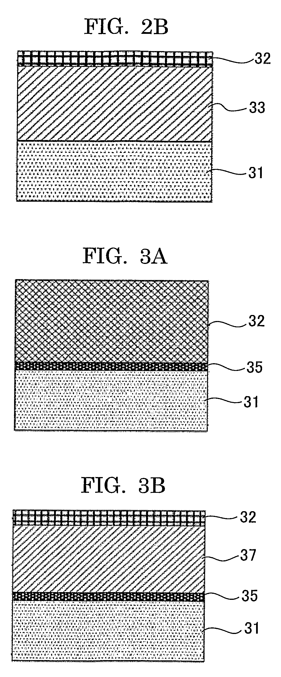
[0330]An undercoat layer of 3.5 μm in thickness, a charge generating layer of 0.2 μm in thickness, and the charge transport layer of 23 μm in thickness were formed on aluminum cylinder of 30 mm in diameter by sequentially applying the coating solution for undercoat layer of the following, applying the coating solution for the charge generating layer of the following, applying the coating solution for the charge transport layer of the following, and followed by drying.

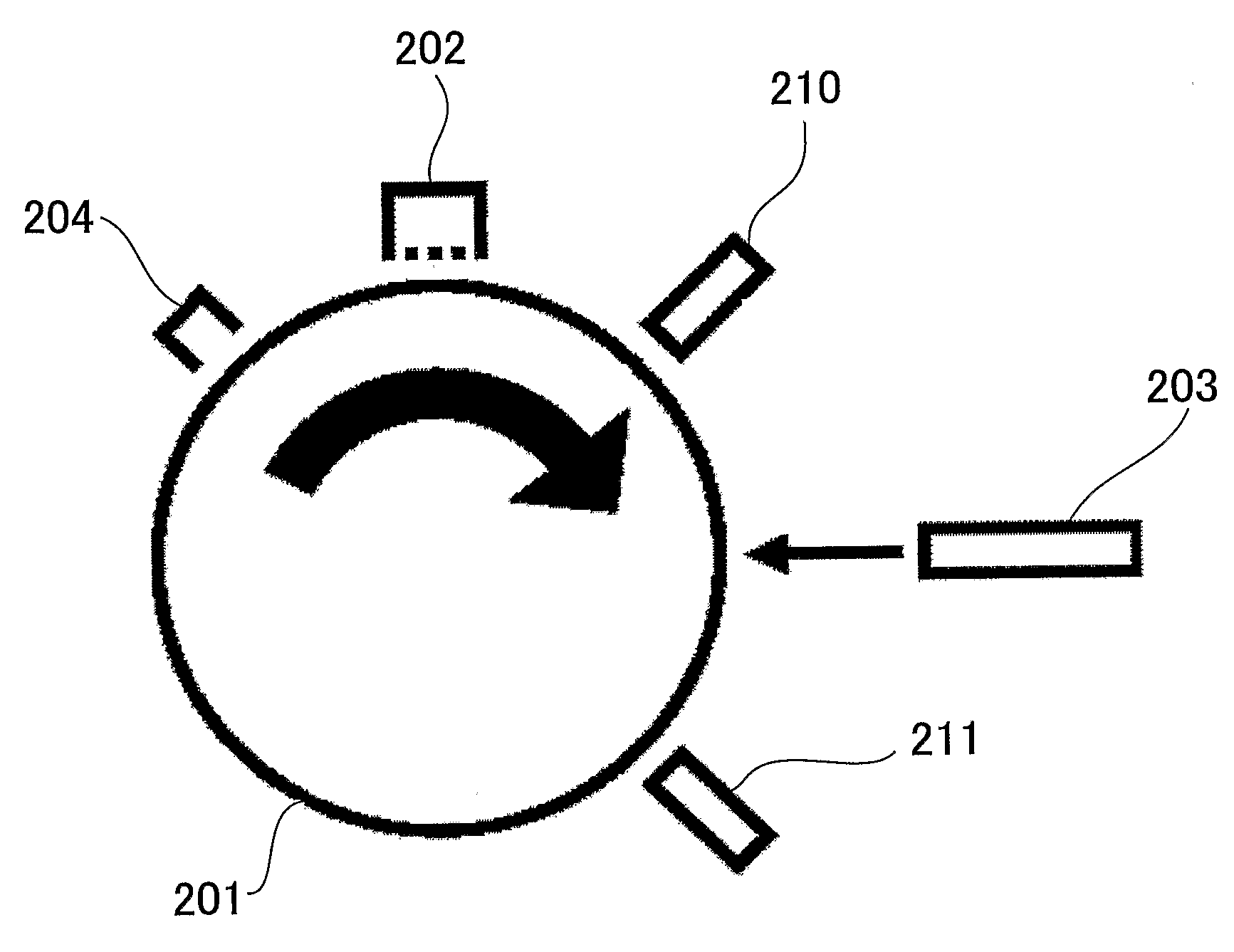
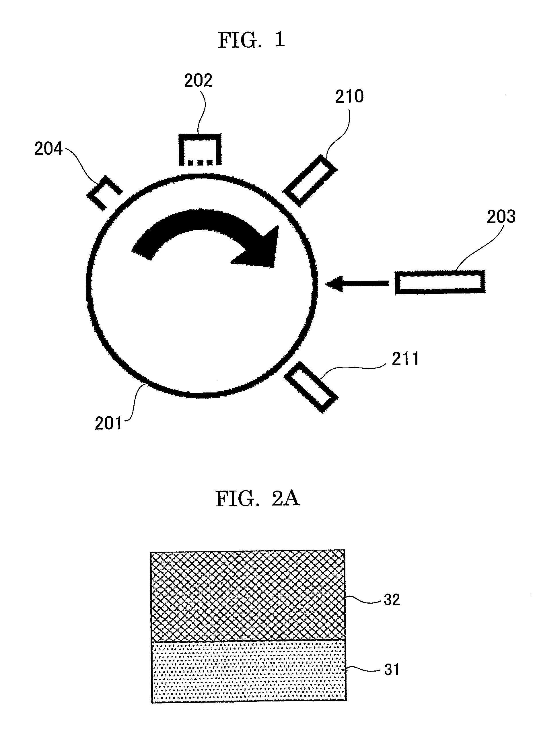
[0331]Then, the surface cross-linked layer of 7 μm in thickness was provided by spray-coating coating solution for a cross-linked surface layer of the following on the charge transport layer, exposing under the condition of 150 sec exposing time by using UV lamp system by Fusion shown in FIG. 6A and UV lamp system by USHIO shown in FIG. 6B, and followed by drying for 20 min at 130° C. Hereinbefore, the electrophotographic photoconductor of Example 1 was produced.

[0332]Here, FIG. 6A shows a (vertical radiation) UV lamp s...

example 2

[0341]An electrophotographic photoconductor of Example 2 was produced similar to that in that in Example 1 except for altering the composition to the following of the coating solution for a cross-linked surface layer, exposure condition, and the method for controlling temperature for Example 1.

[0342]

[Coating Solution for a Cross-Linked Surface Layer]A radically polymerizable compound with charge transport10 partsstructureExample compound No. 180 (molecular weight: 591, numberof functional groups: 2)Radically polymerizable monomer with no charge transport10 partsstructureDipentaerythrytolhexalcrylate (by Nippon Kayaku Co., Ltd.,KAYARAD DPHA, average molecular weight: 536, number offunctional groups: 5.5)Photopolymerizable initiator 1 partIRGACURE 2959 (by Nippon Kayaku Co., Ltd., molecularweight: 224)SolventTetrahydrofuran60 parts(boiling point: 66° C., saturated vapor pressure:176 mmHg / 25° C.)Cyclohexanone60 parts(boiling point: 156° C., saturated vapor pressure:3.95 mmHg / 25° C.)

[Ex...

example 3

[0347]The electrophotographic photoconductor of Example 3 was produced similar to that in Example 1 except for altering the composition to the following of the coating solution for a cross-linked surface layer, exposure condition, and the method for controlling temperature

[0348]

[Coating Solution for a Cross-Linked Surface Layer]A radically polymerizable compound with charge transport10partsstructureExample compound No. 105 (molecular weight: 445,number of functional groups: 1)Radically polymerizable monomer with no charge transportstructureDipentaerythrytolhexyacrylate (by Nippon Kayaku Co.,5partsLtd., KAYARAD DPHA, average molecular weight: 536,number of functional group: 5.5)Trimethylol propane trimethacrylate (by Kayaku Sartomer,5partsSR-350, average molecular weight: 338, number offunctional groups: 3)Photopolymerizable initiators1partKAYACURE CTX (by Nippon Kayaku Co., Ltd.,molecular weight: 204)Solvent120partsTetrahydrofuran (boiling point: 66° C., saturated vaporpressure: 176...


PUM

PropertyMeasurementUnit
surface temperatureaaaaaaaaaa
electrical potentialaaaaaaaaaa
surface temperatureaaaaaaaaaa

Abstract

To provide an electrophotographic photoconductor that comprises a support and a cross-linked layer formed over the support, wherein the cross-linked layer comprises at least light curable of radically polymerizable compound, the difference of maximum value of the post-exposure electrical potential and minimum value of the post-exposure electrical potential when writing is conducted under the condition that image static power is 0.53 mW, exposure energy is 4.0 erg / cm2 for the electrophotographic photoconductor is within 30V.

Description

TECHNICAL FIELD[0001]The present invention relates to a long-lived, high-end electrophotographic photoconductor (hereinafter may be referred to as “photoconductor,”“latent electrostatic image bearing member” or “image bearing member”) that can provide high-quality image formation for prolonged periods, a method for producing the electrophotographic photoconductor, an image forming method, van image forming apparatus, and a process cartridge.BACKGROUND ART[0002]Recently, organic photoconductors (OPC) have been replacing inorganic photoconductor for their excellent performance and various advantages, and are often applied to copiers, facsimile machines, laser printers and complex machines thereof. Examples of the reasons for this include (1) optical property such as a wide range of the wavelength of light absorption and a large amount of light absorption, (2) electric property of high sensitive and stable charging property, (3) a wide range of material selection, (4) easiness to produ...

Claims


Application Information

Patent Timeline
Patent Type & Authority Patents(United States)
IPC IPC(8): G03G17/06
CPCG03G5/0546G03G5/0567G03G5/0592G03G5/14734G03G5/1476G03G5/14791G03G5/005G03G5/0539G03G5/14726G03G5/0525G03G5/142G03G2215/0129
Inventor YANAGAWA, YOSHIKIKAWASAKI, YOSHIAKISUZUKI, TETSURO
Owner RICOH KK
Learn More