
Oxide semiconductor device with oxide semiconductor layers of different oxygen concentrations and method of manufacturing the same
a semiconductor and oxide semiconductor technology, applied in semiconductors, semiconductor devices, electrical equipment, etc., can solve the problems of difficult to use a—si for a thin-film transistor for organic el, oxide semiconductor are not fully used, and good contact properties cannot be obtained, so as to achieve significant improvement of threshold potential shift, high oxygen content ratio, and large threshold potential shift
- Summary
- Abstract
- Description
- Claims
- Application Information
AI Technical Summary
Benefits of technology
Problems solved by technology
Method used
Image

Examples
first embodiment
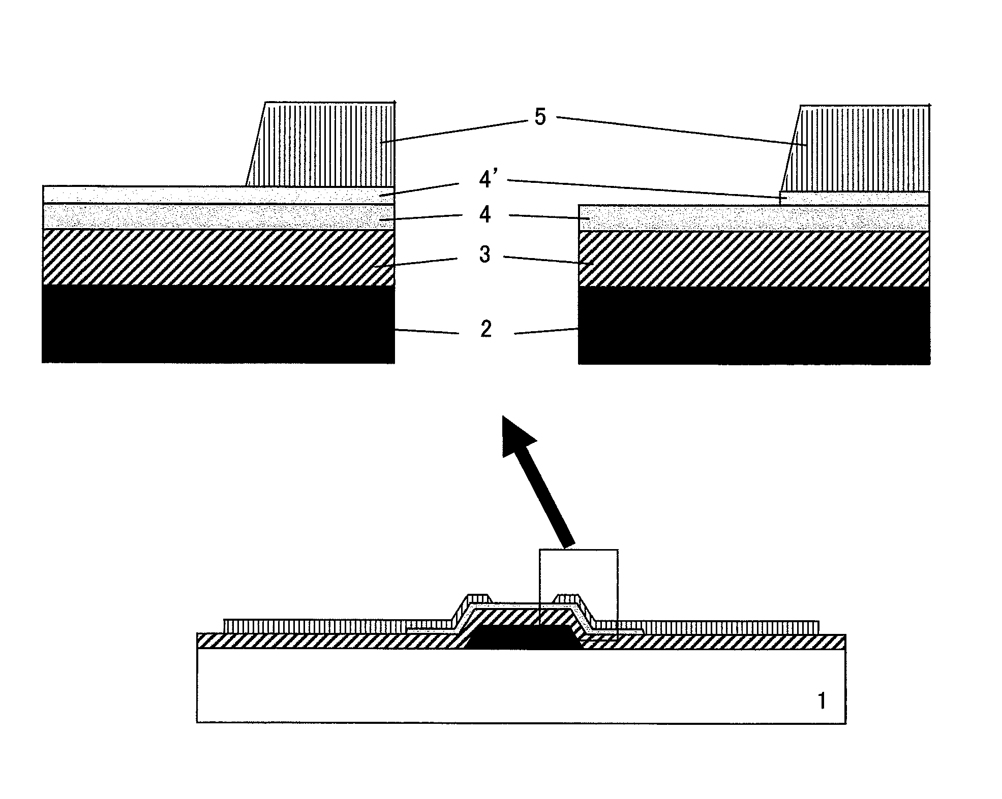
[0037]A structure of a thin-film transistor for an image device according to a first embodiment of the present invention, a method of manufacturing the same, and a method of employing the device and method will be described with reference to FIGS. 7A to 10C. FIGS. 7A to 7E illustrate cross-sectional views of a bottom-gate top-contact thin-film transistor and also flow diagrams illustrating one example of a method of manufacturing the transistor. FIGS. 8 and 9 illustrate a simple configuration of an active-matrix circuit for employing the transistor to a device and a schematic view of the active-matrix circuit, respectively. FIG. 10 is a cross-sectional view illustrating a structure of a thin-film transistor having a structure other than the bottom-gate top-contact structure.
[0038]First, there is prepared a supporting substrate 1 such as, for example, a glass substrate, a quartz substrate, a sapphire substrate, a resin substrate, or a film. Next, there is formed a stacked film of met...
second embodiment
[0044]A structure of an oxide semiconductor thin film memory according to a second embodiment of the present invention and a method of manufacturing the same will be described with reference to FIGS. 11A to 16. FIGS. 11A-11E and 12 illustrate cross-sectional views of an oxide semiconductor thin film memory using a bottom-gate top-contact thin-film transistor according to the present invention and flow diagrams illustrating one example of a manufacturing process of the memory. FIG. 13A illustrates a memory structure including a capacitor on the drain side and FIG. 14A illustrates a memory configuration for performing a memory operation by a change of a gate capacitance, and FIG. 13B and FIG. 14B illustrate cross-sectional views of these memory devices, respectively. FIGS. 15A and 15B are cross-sectional views each illustrating one example of integrating a display-driving transistor using the bottom-gate top-contact thin-film transistor according to the method of the present invention...
third embodiment
[0050]A structure of a touch panel using an oxide semiconductor thin-film transistor according to a third embodiment of the present invention and a method of manufacturing the same will be described with reference to FIGS. 17A-17D and 18. FIGS. 17A-17D are cross-sectional views of an oxide semiconductor touch panel (touch sensor) according to the present invention and flow diagrams illustrating one example of a manufacturing process of the oxide semiconductor touch panel. FIG. 18 is a cross-sectional view illustrating one example in which the oxide semiconductor touch panel and the oxide semiconductor transistor according to the present invention are integrated as a back-emission type organic EL display.
[0051]Although a basic structure of the touch panel according to the present invention is almost the same with that of the oxide semiconductor thin-film transistor array described in the second embodiment, no surface unevenness is desirable in a surface of the structure of the touch ...
PUM
| Property | Measurement | Unit |
|---|---|---|
| band gap | aaaaa | aaaaa |
| threshold potential | aaaaa | aaaaa |
| thickness | aaaaa | aaaaa |
Abstract
Description
Claims
Application Information