

Gallium nitride crystal growth method, gallium nitride crystal substrate, epi-wafer manufacturing method, and epi-wafer
a gallium nitride and crystal growth technology, applied in the direction of crystal growth process, polycrystalline material growth, chemically reactive gas, etc., can solve the problems of low oxide generation, low yield, and high cost, and achieve the effect of a large thickness
- Summary
- Abstract
- Description
- Claims
- Application Information
AI Technical Summary
Benefits of technology
Problems solved by technology
Method used
Image

Examples
embodiment mode 1
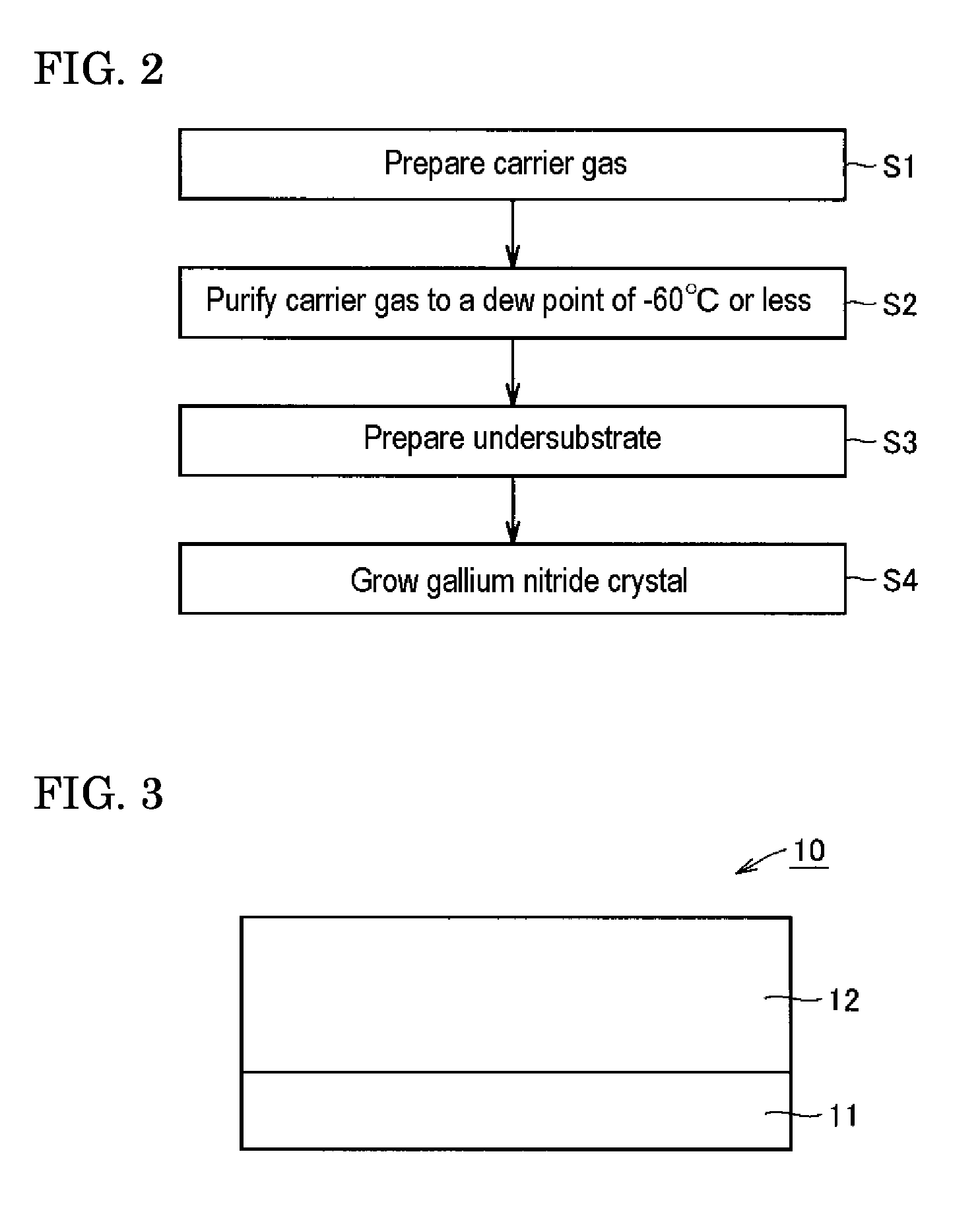
[0036]A gallium nitride crystal growth method in one embodiment mode of the present invention will be explained. In the gallium nitride crystal growth method in this embodiment mode, carrier gases, gallium nitride precursors, and a gas containing silicon as a dopant are employed to grow gallium nitride crystal onto an undersubstrate by hydride vapor phase epitaxy (HVPE).
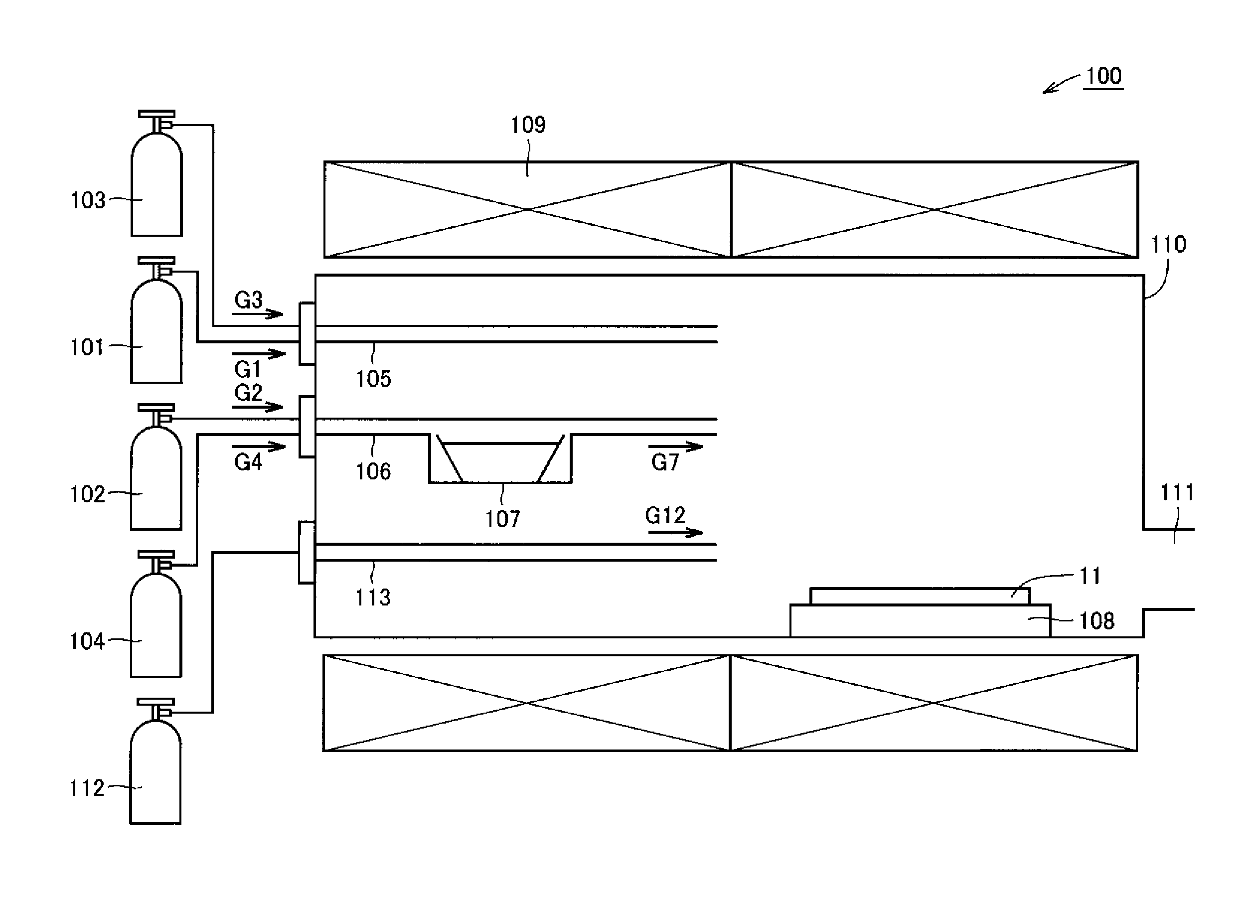
[0037]FIG. 1 is an outline diagram illustrating a HVPE reactor employed in the gallium nitride crystal growth method in the one embodiment mode of the present invention. First, referring to FIG. 1, a HVPE reactor 100 employed in the gallium nitride crystal growth method in this embodiment mode will be explained. As illustrated in FIG. 1, the HVPE reactor 100 is provided with a first source-gas cylinder 101, second source-gas cylinder 102, first-carrier-gas cylinder 103, second-carrier-gas cylinder 104, first gas introducing line 105, second gas introducing line 106, source boat 107, susceptor 108, heater 109, crystal...
embodiment mode 2
[0061]FIG. 4 is a flow chart representing an epi-wafer manufacturing method in Embodiment Mode 2. FIG. 5 is a schematic diagram illustrating a substrate in Embodiment Mode 2. FIG. 6 is a schematic diagram illustrating an epi-wafer in Embodiment Mode 2. Referring to FIGS. 4 through 6, an epi-wafer manufacturing method in this embodiment mode will be explained.
[0062]First, gallium nitride crystal 12 is grown onto an undersubstrate 11 by the gallium nitride crystal growth method in Embodiment Mode 1 (S1 to S4). As a result, gallium nitride crystal substrate 10 as illustrated in FIG. 3 is obtained.
[0063]Next, as represented and illustrated in FIGS. 4 and 5, at least the undersubstrate 11 is removed from the gallium nitride crystal substrate 10 to form a substrate 20 consisting of the gallium nitride crystal 12 (Step S5). In the proximity of the interface between gallium nitride crystal 12 and undersubstrate 11, crystallinity is often unfavorable. Therefore, the region in the gallium nit...
embodiments
[0073]In the present embodiments, effects of employing a carrier gas having a dew point of −60° C. or less to grow gallium nitride crystal were investigated. Specifically, epi-wafers of Embodiments 1 through 15 and of Comparative Examples 1 through 3 were each produced to measure in the epi-wafers incidence of cracking, and the extent to which operating voltage rose.
PUM
| Property | Measurement | Unit |
|---|---|---|
| dew point | aaaaa | aaaaa |
| thickness | aaaaa | aaaaa |
| length | aaaaa | aaaaa |
Abstract
Description
Claims
Application Information