Clock network fishbone architecture for a structured ASIC manufactured on a 28 NM CMOS process lithographic node

a technology of structured asics and fishbones, which is applied in the direction of power consumption reduction, pulse technique, generating/distributing signals, etc., can solve the problems of wasting significant power in transitions within blocks, consuming time and effort, and limiting the maximum performance of the entire system

Inactive Publication Date: 2014-01-14
INTEL CORP
View PDF1 Cites 46 Cited by
  • Summary
  • Abstract
  • Description
  • Claims
  • Application Information

AI Technical Summary

Benefits of technology

[0047]Another aspect of the present invention is to provide a clock tree that has a low-level clock mesh of a beneficial fishbone construction.
[0048]Still another aspect of the present inventio

Problems solved by technology

While the layout of each cell in a standard cell is predetermined, the circuit itself has to be uniquely constructed by connecting all layers to one another and the cells within each layer in a custom manner, which takes time and effort.
The control of any differences and uncertainty in the arrival times of the clock signals can limit the maximum performance of the entire system and create race conditions in which an incorrect data signal may latch within a register.
The clock distribution network often takes a significant portion of the power consumed by a chip; furthermore, significant power can be wasted in transitions within blocks, when their output is not needed.
A simple PLD, historically called a programmable logic device, is much more limited in application, as they do not have a general interconnect structure.
These components are no longer supported by modern EDA (Electronic Design Automation) software and have very limited functionality.
However, optimizing multilevel synthesis logic is more difficult than optimizing two-level synthesis logic, and often employs heuristic techniques.
Design constraints in floorplanning include minimizing the silicon chip area and minimizing timing delay.
The determination of the MRST is in general a NP-complete problem—which is difficult to solve in a reasonable time.
For small numbers of terminals heuristic algorithms exist, but they are expensive in engineering cost to compute.
If a via is disabled, then it cannot practically conduct a signal, i.e., the via has very high resistance or does not physically exist.
If the clock signal arrives at different components at different times, there is clock skew.
Clock skew can be caused by many different things, such as wire-interconnect length, temperature variations and differences in input capacitance on the clock inputs of devices using the clock.
These are also the disadvantages of standard cell ASICs: they can be difficult to design, have longer development times, and high

Method used


Image

  • Clock network fishbone architecture for a structured ASIC manufactured on a 28 NM CMOS process lithographic node
  • Clock network fishbone architecture for a structured ASIC manufactured on a 28 NM CMOS process lithographic node
  • Clock network fishbone architecture for a structured ASIC manufactured on a 28 NM CMOS process lithographic node

Examples


Embodiment Construction

[0069]The method and apparatus of the present invention may be described in software, such as the representation of the invention in an EDA tool, or realized in hardwire, such as the actual physical instantiation.

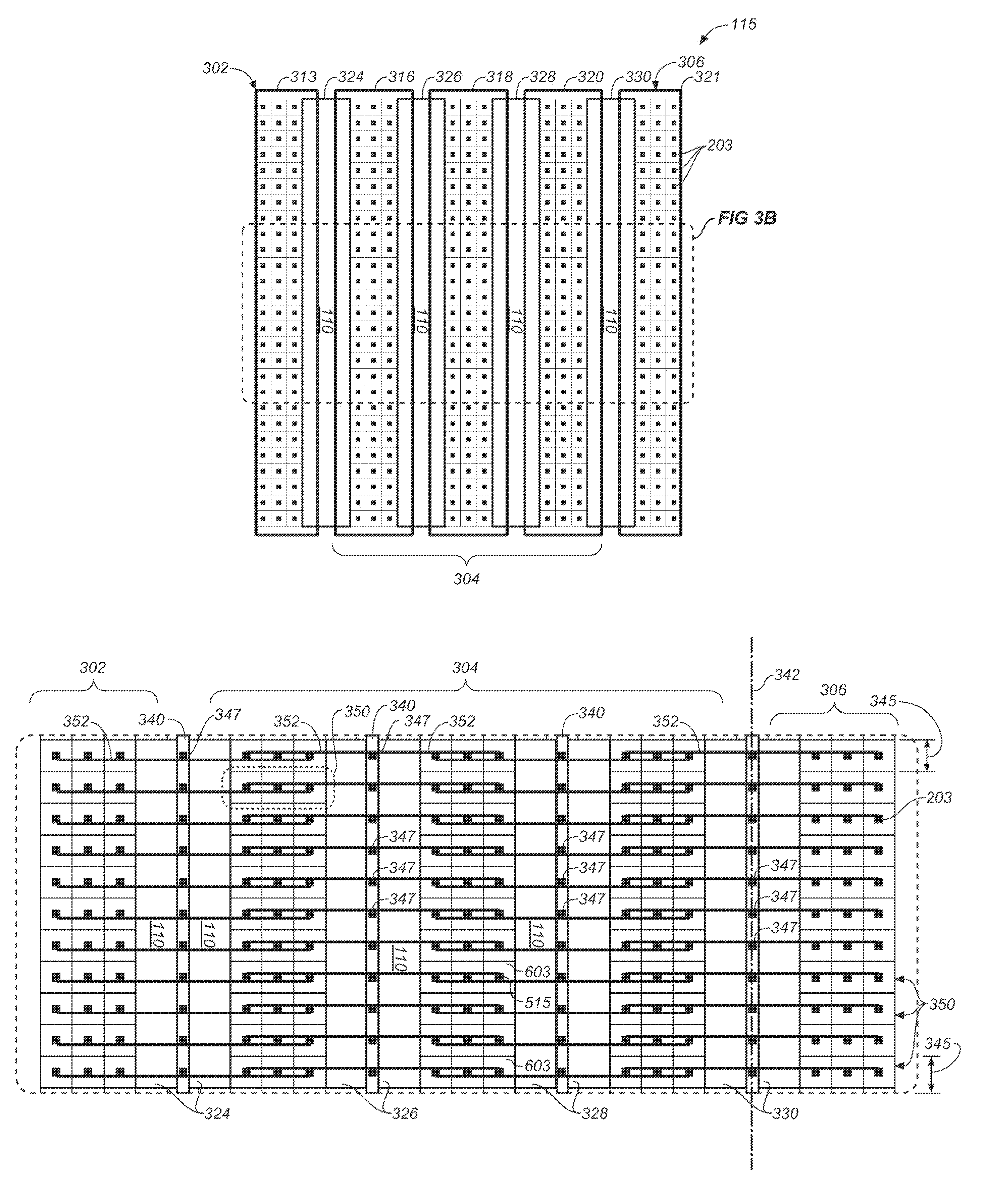
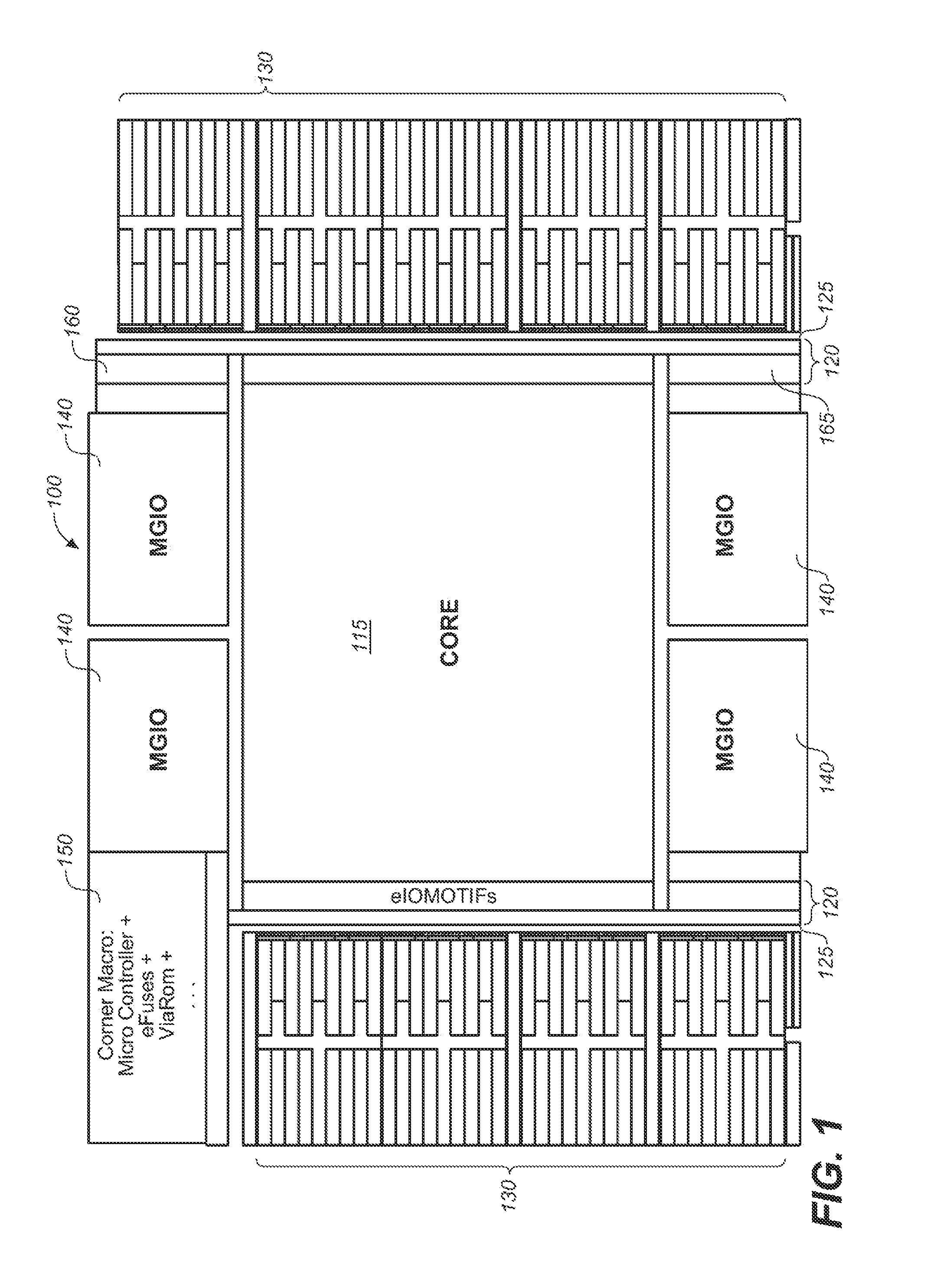
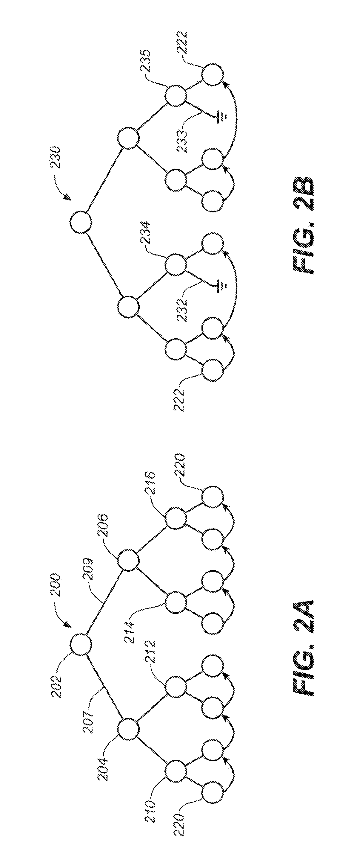
[0070]Regarding the floorplan of the present invention, the drawings sometimes show elements as blocks that in a physical implementation may differ from this stylized representation, but the essential features of the floorplan should be apparent to one of ordinary skill in the art from the teachings herein. The exact placement of the blocks vis-à-vis neighboring blocks can vary in an actual chip from the simple stylized representations as shown in the figures, and in addition there may be several layers in an ASIC chip that achieve the functionality shown, superimposed on one another, and not necessarily a single layer as shown in the drawings. This is true for most of the elements in the present invention, as understood by one of ordinary skill, and that does not detract f...


PUM


Abstract

A clock architecture for a Structured ASIC chip, manufactured using a CMOS process is shown. A via-configurable logic block (VCLB) architecture in the Structured ASIC has a core region containing memory and logic cells arranged in columns that are supplied by a clock network having a global clock network tree and a low-level clock mesh to distribute the global clock signal in a repeating pattern. The clock mesh has a fishbone configuration in outline and allows for scalable expansion of the clock network. In one embodiment 36 global clocks may be provided to the Structured ASIC, with four clocks per logic cell. The VCLB Structured ASIC chip is manufactured on a 28 nm CMOS process lithographic node, having several metal layers but preferably is programmable on a single via layer.

Description

CROSS-REFERENCE TO RELATED APPLICATIONS[0001]The present application is related to: U.S. application Ser. No. 13 / 649,510, for “VIA-CONFIGURABLE HIGH-PERFORMANCE LOGIC BLOCK INVOLVING TRANSISTOR CHAINS” by Andrew Andreev, Sergery Gribok, Ranko Scepanovic, Phey-Chuin TAN, Chee-Wei KUNG, filled the same day as the present invention, Oct. 11, 2012; U.S. application Ser. No. 13 / 649,529, for “ARCHITECTURAL FLOORPLAN FOR A STRUCTURED ASIC MANUFACTURED ON A 28 NM CMOS PROCESS LITHOGRAPHIC NODE OR SMALLER” by Alexander Andreev, Ranko Scepanovic, Ivan Pavisic, Alexander Yahontov, Mikhail Udovikhin, Igor Vikhliantsev, Chong-Teik LIM, Seow-Sung LEE, Chee-Wei KUNG, filed the same day as the present invention, Oct. 11, 2012; U.S. application Ser. No. 13 / 649,551, for MICROCONTROLLER CONTROLLED OR DIRECT MODE CONTROLLED NETWORK-FABRIC ON A STRUCTURED ASIC” by Alexander Andreev, Andrey Nikitin, Marian Serbian, Massimo Verita, filed the same day as the present invention, Oct. 11, 2012; U.S. applicati...

Claims


Application Information

Patent Timeline
IPC IPC(8): H01L23/52
CPCH01L23/52H01L2924/0002G06F1/10H03K19/1774H03K19/0013H03K19/0016H01L2924/00
Inventor ANDREEV, ALEXANDERNIKISHIN, ANDREYGRIBOK, SERGEYTAN, PHEY-CHUINCHOO, CHOON-HUN
Owner INTEL CORP
Why Eureka
Try Eureka