Optical coupling device having KBBF group crystal coupled with prisms and method for manufacturing same

a technology of optical coupling and prism, which is applied in the field of optical couplers, can solve the problems of affecting the quality of devices, affecting the bonding strength of the present invention, and difficulty in achieving an optical adhesive whose refractive index completely consists with that of the optical components, etc., and achieves enhanced optical contact, improved bonding strength, and simple process

Inactive Publication Date: 2014-07-08
TECHNICAL INST OF PHYSICS & CHEMISTRY - CHINESE ACAD OF SCI
View PDF4 Cites 7 Cited by
  • Summary
  • Abstract
  • Description
  • Claims
  • Application Information

AI Technical Summary

Benefits of technology

[0011]The present invention has been made to overcome the above problem that the bonding force of optical contact is insufficient between the KBBF family crystal and prisms of the existing KBBF family crystal-prism coupler by providing a KBBF family nonlinear optical crystal-prism coupler and its fabrication method. Here, the KBBF family crystal and the prisms are coupled by optical contact through transition layers, which belongs to bonding between the same type of materials. This could intensify the ability of bonding. Furthermore, there is no cavity in the bonding region and the bonding strength is enhanced enormously. The present invention is achieved by a simple process with low cost. It can be applied to fabricate laser optical components to improve the device performance and the laser damage resist threshold.
[0046]bonding one of the first transition layers deposited on the KBBF family crystal and the second transition layer of the respective prism by optical contact, bonding the other first transition layer and the second transition layer of the other prism by optical contact, and then heating the bonded crystal-prism coupler at an elevated temperature to ensure that the crystal and the prisms are bonded to each other firmly, thereby achieving the KBBF family nonlinear optical crystal-prism coupler,
[0052]In the present invention, the KBBF family crystal and the prisms are coupled together by optical contact through transition layers, which belongs to the optical contact between the same materials. In this way, the present invention provides a stronger ability for optical contact, giving a bonding force larger than that from normal optical direct bonding.
[0055]The present invention provides a KBBF family nonlinear optical crystal-prism coupler and its fabrication method. Such an optical contact with transition layers used by the invention can be referred to as “deeply optical contact”. The present invention is advantageous in that an enhanced optical contact is achieved and there has no cavity in the bonding area as to a KBBF family crystal and other optical crystal or optical glass, or a KBBF family crystal and a KBBF family crystal. The bonding strength of the present invention is greatly improved than common optical contact. Furthermore, the present invention employs a simple process with low cost. It can be used to fabricate laser optical components to reduce thermal effect, improve the device performance and the laser damage resist threshold.

Problems solved by technology

There is a disadvantage that any intermediate bonding material may form flaw and stains on the surfaces, affecting the quality of devices.
Furthermore, it is difficult to achieve an optical adhesive of which refractive index completely consists with that of the optical components, especially when the two optical components are different optical materials.
Light unavoidably suffers Fresnel reflection and thus loses light flux while travelling through interfaces of the components and adhesive.
Finally, a bonding force of optical adhesive is insufficient.
Especially, the optical adhesive is liable to be softened, deformed and even crack under heat in a laser system.
However, if the two optical components for bonding are of different optical materials or of the same optical material with different surface structures, inconsistent expansion will result in the separation of the two components due to the difference in thermal expansion coefficient when the interface is heated.
In view of the above, optical direct bonding between different materials is generally limited to be used in a low-power laser system.
Therefore, the two optical components may suffer different thermal expansions to be separated or appear interface damage.
Especially, a high-power laser system has high laser power, long duration, poor heat dissipation at the interface, and is generally damaged primarily at the interface due to over-high temperature.
As a result, laser beam quality degrades, and the two interfaces may separate from each other to cause the high-power laser system disable.
Further, compose of the KBBF family crystal is complex and there are many atomic species.
Accordingly, the KBBF family crystal has complex thermal property, which is also called as poor optical contact ability.
In the high-power laser system, the interfaces are also damaged at first and the two interfaces separate from each other if it is worse.

Method used


Image

  • Optical coupling device having KBBF group crystal coupled with prisms and method for manufacturing same
  • Optical coupling device having KBBF group crystal coupled with prisms and method for manufacturing same
  • Optical coupling device having KBBF group crystal coupled with prisms and method for manufacturing same

Examples


embodiment 1

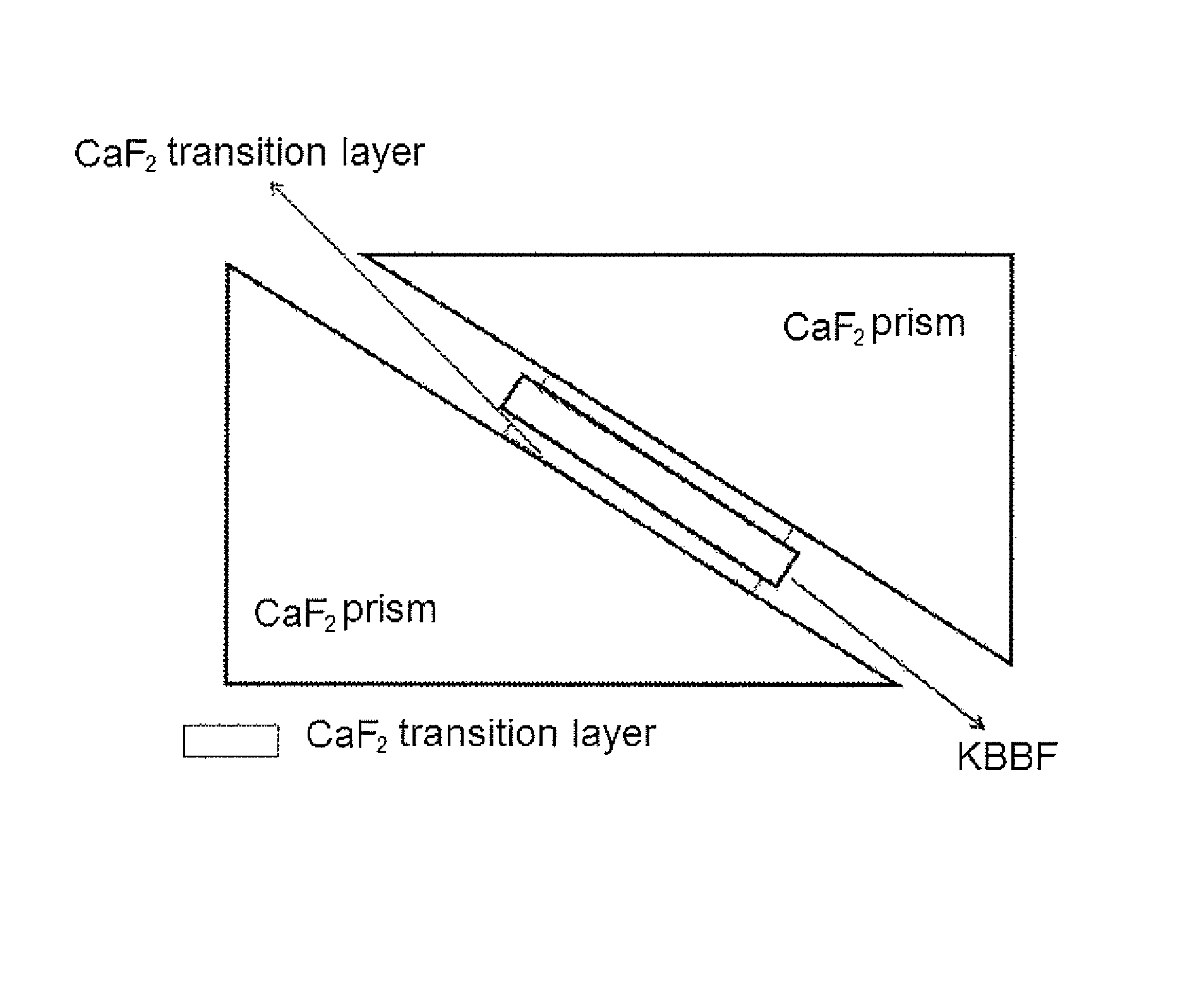
The Fabrication of a KBBF-Calcium Fluoride (CaF2) Crystal-Prism Coupler

[0059]The KBBF-CaF2 crystal-prism coupler for coherent light output of 177.3 nm shown in FIG. 1 is fabricated by the following process.

[0060]First of all, two optical contact surfaces of a KBBF family crystal and optical contact surfaces of two CaF2 prisms are polished precisely to form ultra-smooth surfaces. The smooth surfaces of the KBBF family crystal and the prisms have surface roughness Ra of less than 0.5 nm and surface flatness of less than ⅛λ (λ=632.8 nm).

[0061]Each of both polished surfaces of the KBBF family crystal is then deposited respectively by a layer of CaF2 film, which has a thickness in a range of 200 nm-250 nm. Vapor deposition is applied to the CaF2 film by ion beam assisted electron beam evaporation. After activating the CaF2 coatings by mechanical polishing, the two coated surfaces of KBBF crystal bond with CaF2 crystal prisms by optical contact. The bonded KBBF-CaF2 crystal-prism coupler ...

embodiment 2

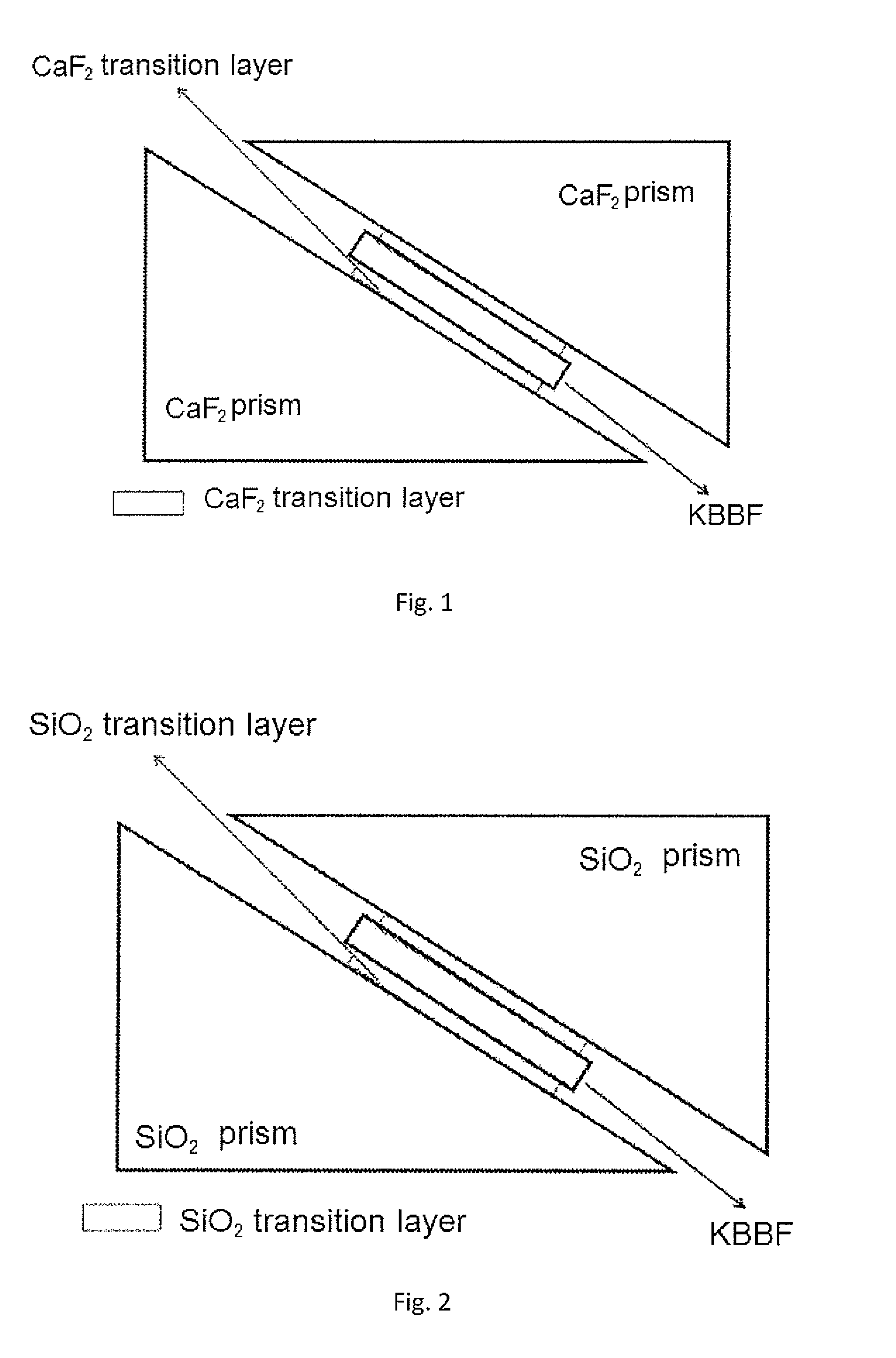
The Fabrication of a KBBF-Fused Silica (SiO2) Prism Coupler

[0062]The KBBF-fused silica prism coupler for coherent light output of 193 nm shown in FIG. 2 is fabricated by a way similar to Embodiment 1. The difference is in that the transition layers deposited on the surfaces of KBBF crystal are SiO2 films and both fused silica prisms are SiO2 films. The SiO2 films are in thickness of 300 nm-320 nm. Vapor deposition is applied to the SiO2 films by ion beam assisted electron beam evaporation. The four SiO2 films coated on the KBBF crystal and fused silica prisms are activated by mechanical polishing. The KBBF crystal then optically contacts with fused silica glass prisms (with composition of SiO2) through SiO2 films on respective surfaces. The bonded crystal-prism coupler is clamped firmly at two ends with a certain force by a clamp. After that, the coupler is heated in a furnace at 100° C. for 80 hours in an atmosphere of argon. The KBBF-fused silica prism coupler in this embodiment i...

embodiment 3

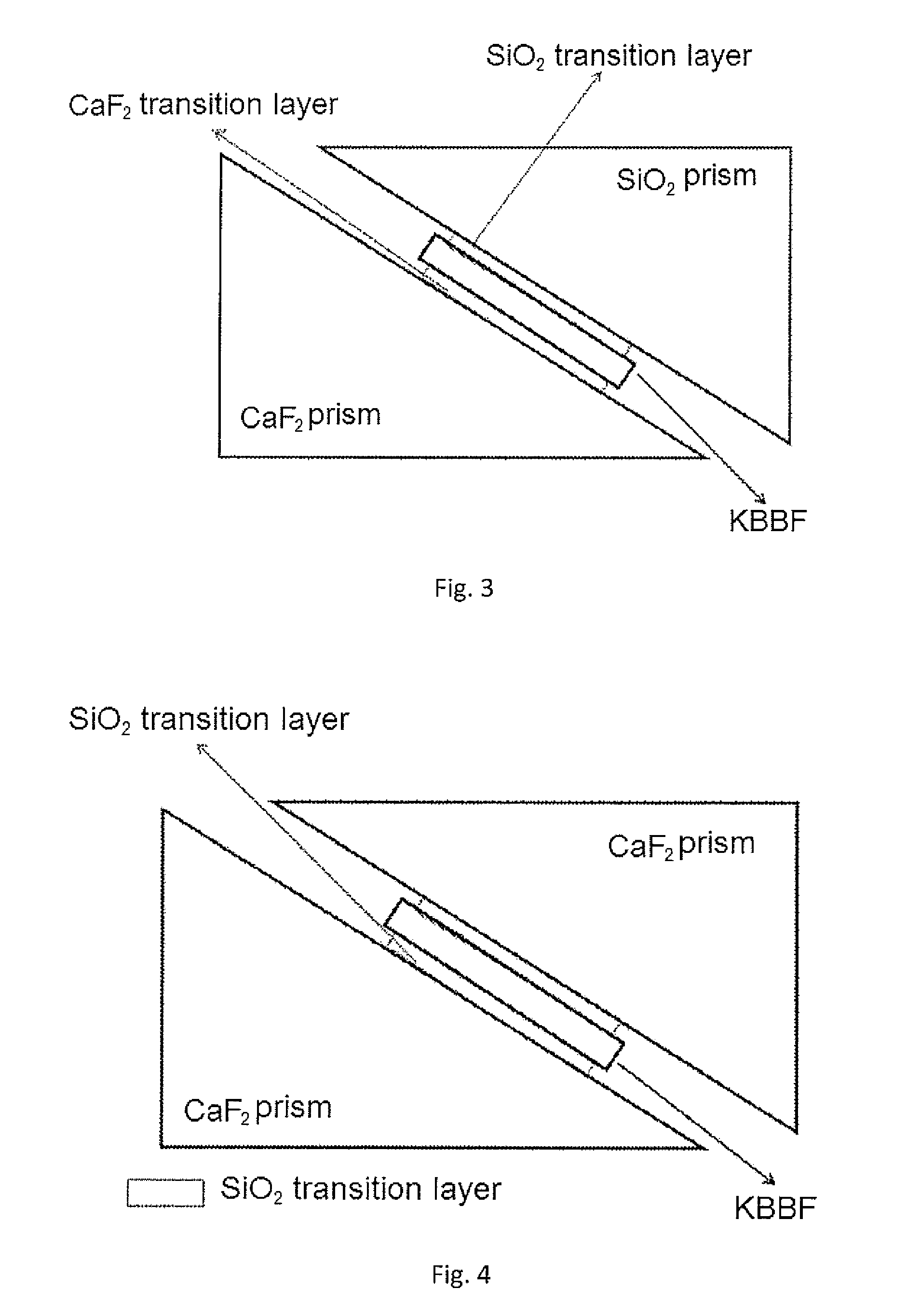
The Fabrication of a KBBF-CaF2 / SiO2 Prism Coupler

[0063]The KBBF-CaF2 / SiO2 prism coupler for coherent light output of 177.3 nm shown in FIG. 3 is fabricated by a way similar to Embodiment 1. Embodiment 3 is different from Embodiment 1 in that: one of the transition layers deposited on one of the two surfaces of the KBBF crystal is CaF2 film, and the other transition layer deposited on the other surface of the KBBF crystal is SiO2 film; a CaF2 film and a SiO2 film are coated on the CaF2 prism and the SiO2 prism, respectively; the CaF2 films are in thickness of 500 nm-550 nm and the SiO2 films are in thickness of 600 nm-700 nm. Vapor deposition is applied to the CaF2 and SiO2 films by ion beam assisted electron beam evaporation. The deposited CaF2 films and SiO2 films are activated by plasma, then one surface of the KBBF crystal optically contacts with the CaF2 crystal prism through the CaF2 films, the other surface of the KBBF crystal optically contacts with the fused silica glass (wi...


PUM

PropertyMeasurementUnit
surface flatnessaaaaaaaaaa
poweraaaaaaaaaa
poweraaaaaaaaaa

Abstract

The present invention relates to a KBBF family nonlinear optical crystal-prism coupler and its method of fabrication. The coupler comprises: a KBBF family crystal with two smooth surfaces; transition layers each of which is deposited on respective one of the two smooth surfaces of the KBBF family crystal; and a pair of prisms each of which optically contacts with respective one of the activated transition layers. The present invention further provides a KBBF family nonlinear optical crystal-prism coupler that comprises: a KBBF family crystal with two smooth surfaces; a pair of prisms each of which has a smooth surfaces; first transition layers each of which is deposited on respective one of the two smooth surfaces of the KBBF family crystal; and second transition layers each of which is deposited on a smooth surface of respective one of the pair of prisms, wherein the first and second transition layers are integral by optical contact. The coupling between the KBBF family crystal and the prisms is achieved by optical contact through transition layers to improve bonding strength.

Description

CROSS-REFERENCE TO RELATED APPLICATION(S)[0001]This application is a National Phase Patent Application and claims priority to and benefit of International Application Number PCT / CN2012 / 000355, filed on Mar. 21, 2012, which claims priority to and benefit of Chinese Patent Application Number 201110112761.2, filed on May 3, 2011, the entire disclosures of which are incorporated herein by reference.BACKGROUND OF THE INVENTION[0002]1. Field of the Invention[0003]The present invention relates to an optical coupler, especially to a KBBF family nonlinear optical crystal-prism coupler.[0004]2. Description of the Related Art[0005]Two or more optical components are generally bonded together in an optical system. Generally, there are three following methods: optical adhesive bonding, optical direct bonding and diffusion bonding. The optical adhesive bonding bonds two polished mirror surfaces with optical adhesive. This technique is simple and can be used to bond different optical materials. The...

Claims


Application Information

Patent Timeline
Patent Type & Authority Patents(United States)
IPC IPC(8): G02F1/355
CPCG02B5/04G02F1/3551G02B1/02G02F1/3501G02F2001/3503G02F1/353G02F1/3503
Inventor CHEN, CHUANGTIANZHU, YONGFAN, FEIDIWANG, XIAOYANGLI, RUKANG
Owner TECHNICAL INST OF PHYSICS & CHEMISTRY - CHINESE ACAD OF SCI
Why Eureka
Try Eureka