
Gate stacks including TaXSiYO for MOSFETS

a gate stack and mosfet technology, applied in the field of mosfet assembly, can solve the problems of limited success up, significant challenges for fets in particular, and the scaling and performance improvement requirements of semiconductor devices, and achieve the effect of reducing the overall pressure of the environmen

Inactive Publication Date: 2015-03-10
INTERMOLECULAR
View PDF11 Cites 0 Cited by
  • Summary
  • Abstract
  • Description
  • Claims
  • Application Information

AI Technical Summary

Benefits of technology

This patent is about a process for making a structure with a dielectric layer. The process involves forming a layer of titanium nitride over the dielectric layer which prevents oxidation of the tantalum silicon oxide in the dielectric layer. The interface layer is also kept in an oxygen-free environment to maintain the concentration of oxygen and stoichiometry of tantalum silicon oxide. The process ensures that the structure has good quality and performance.

Problems solved by technology

The continuous device scaling and performance improvement requirements of semiconductor devices in general and FETs in particular face significant challenges as conventional silicon-based FETs come to their fundamental physical limits.
Suitable gate dielectrics or passivation layers on III-V compound semiconductors have been researched for more than four decades (since introduction of polysilicon gate in the 1960s) with very limited success up until now.
The saturation during the reaction and purging stages makes the growth self-limiting.

Method used


Image

  • Gate stacks including Ta<sub>X</sub>Si<sub>Y</sub>O for MOSFETS
  • Gate stacks including Ta<sub>X</sub>Si<sub>Y</sub>O for MOSFETS
  • Gate stacks including Ta<sub>X</sub>Si<sub>Y</sub>O for MOSFETS

Examples


Embodiment Construction

[0021]In the following description, numerous specific details are set forth in order to provide a thorough understanding of the presented concepts. The presented concepts may be practiced without some or all of these specific details. In other instances, well known process operations have not been described in detail so as to not unnecessarily obscure the described concepts. While some concepts will be described in conjunction with the specific embodiments, it will be understood that these embodiments are not intended to be limiting.

INTRODUCTION

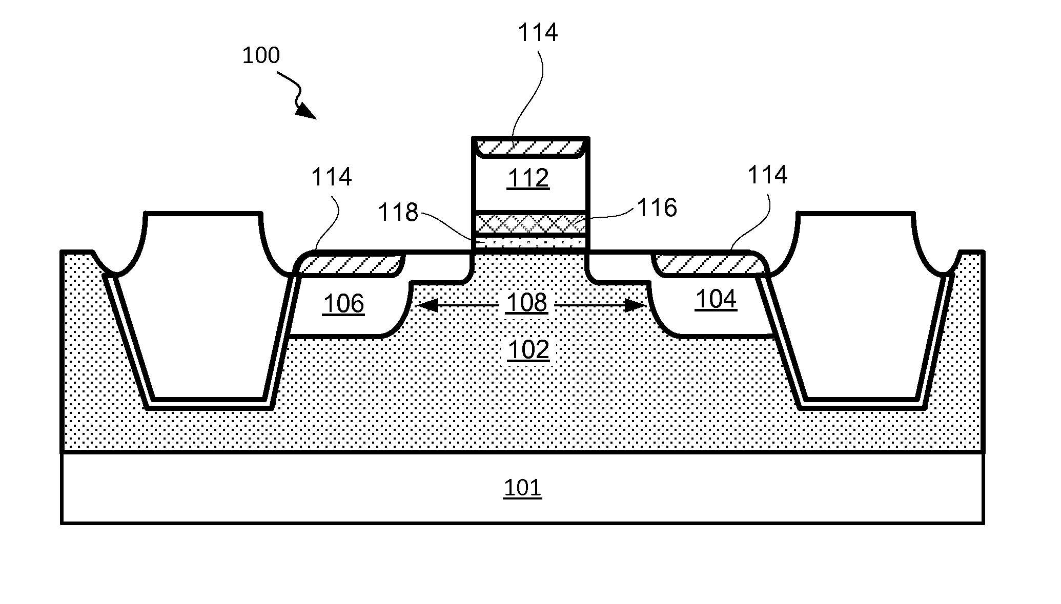
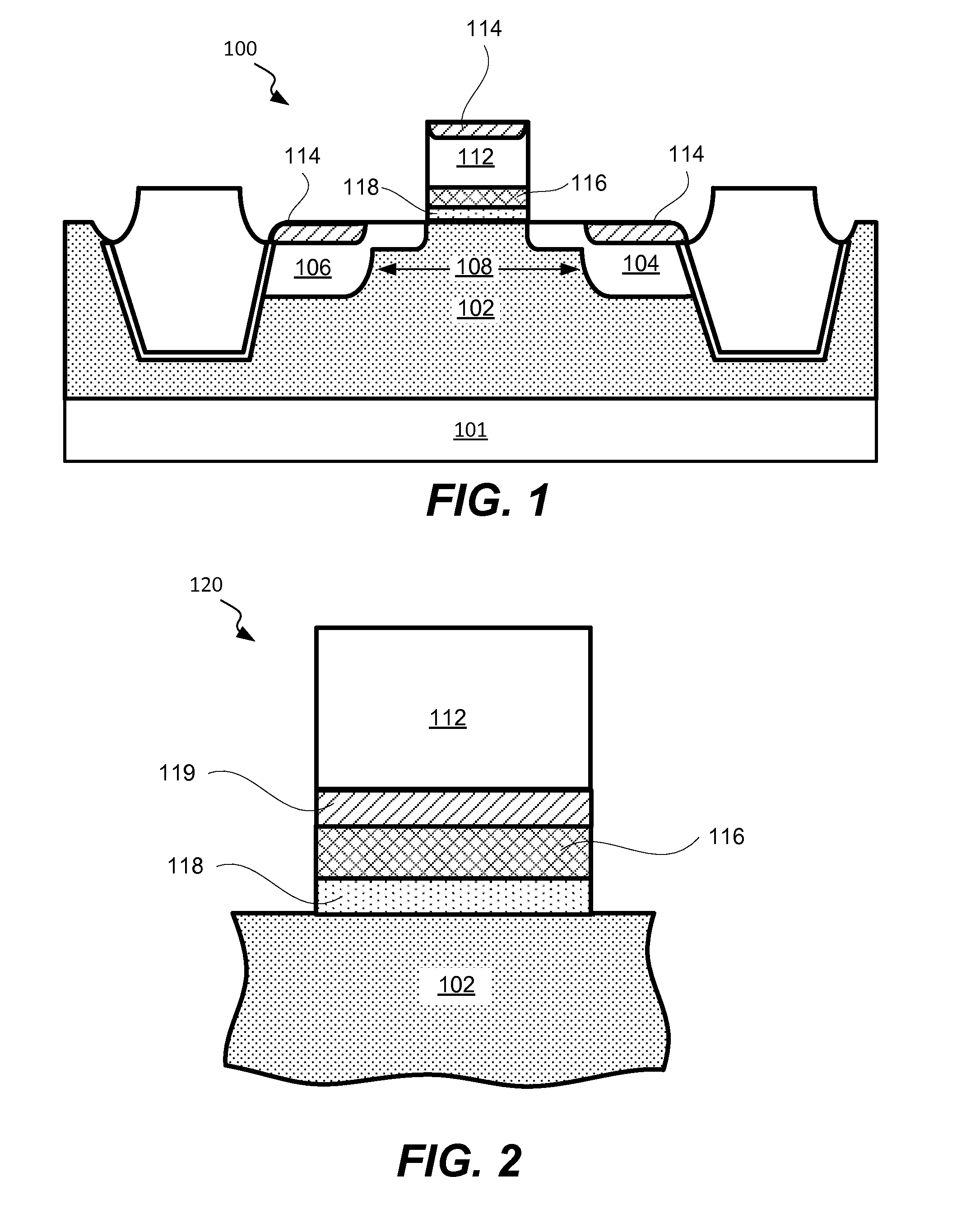
[0022]The continuous device scaling and performance improvement requirements of semiconductor devices in general and FETs in particular face significant challenges as conventional silicon-based FETs come to their fundamental physical limits. As new technologies, such as high-k metal gates, non-planar silicon transistors, and strained channel materials are developed, additional efforts are needed find new channel materials, such as germanium a...


PUM


Abstract

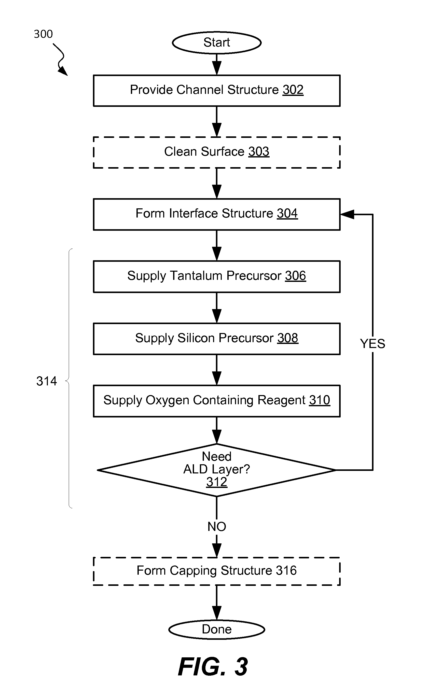
Provided are field effect transistor (FET) assemblies and methods of forming thereof. An FET assembly may include a dielectric layer formed from tantalum silicon oxide and having the atomic ratio of silicon to tantalum and silicon (Si / (Ta+Si)) of less than 5% to provide a low trap density. The dielectric layer may be disposed over an interface layer, which is disposed over a channel region. The same type of the dielectric layer may be used a common gate dielectric of an nMOSFET (e.g., III-V materials) and a pMOSFET (e.g., germanium). The channel region may include one of indium gallium arsenide, indium phosphate, or germanium. The interface layer may include silicon oxide to provide a higher energy barrier. The dielectric layer may be formed using an atomic layer deposition technique by adsorbing both tantalum and silicon containing precursors on the deposition surface and then oxidizing both precursors in the same operation.

Description

CROSS-REFERENCE TO RELATED APPLICATIONS[0001]This application claims priority from U.S. Provisional Application No. 61 / 862,926, filed on 6 Aug. 2013, which is incorporated herein by reference in its entirety for all purposes.TECHNICAL FIELD[0002]The present invention relates generally to field effect transistor (FET) assemblies and more specifically to FET assemblies including gate stacks with tantalum silicon oxide.BACKGROUND[0003]A typical FET assembly includes a gate, a source, and a drain. The gate is conventionally formed from a gate insulator and a gate electrode. The gate insulator may be a layer of silicon oxide (SiO2) or silicon oxynitride (SiON) disposed over a silicon substrate. The gate insulator may be also referred to as a gate dielectric or a gate oxide. The gate electrode may be a layer of poly-crystalline silicon (polysilicon) disposed over the gate insulator. The gate electrode and, optionally, the gate insulator layer may be etched from continuous layers to form a...

Claims


Application Information

Patent Timeline
IPC IPC(8): H01L21/70H01L21/28H01L27/092
CPCH01L21/28158H01L27/092H01L21/28255H01L21/28264H01L29/4966H01L29/513H01L29/517H01L29/665H01L29/6659H01L29/7833H01L29/16H01L29/20H01L21/8258H01L21/0215H01L21/0228
Inventor AHMED, KHALEDGREER, FRANK
Owner INTERMOLECULAR
Learn More