Methods of forming nanoparticles using semiconductor manufacturing infrastructure

a technology of manufacturing infrastructure and nanoparticles, which is applied in the direction of manufacturing tools, microstructure devices, coatings, etc., can solve the problems of not necessarily being suitable for making a semiconductor device, and not necessarily a suitable material for the manufacture of a semiconductor devi

Active Publication Date: 2015-03-24
IBM CORP
View PDF18 Cites 3 Cited by
  • Summary
  • Abstract
  • Description
  • Claims
  • Application Information

AI Technical Summary

Problems solved by technology

Substrate 10 is a substrate suitable for spin casting (e.g., silicon, ceramic, and / or metal wafer), but not necessarily a substrate suitable for making a semiconductor device.
However, the template-forming material is not necessarily a material suitable for the manufacture of a semiconductor device.

Method used


Image

  • Methods of forming nanoparticles using semiconductor manufacturing infrastructure
  • Methods of forming nanoparticles using semiconductor manufacturing infrastructure
  • Methods of forming nanoparticles using semiconductor manufacturing infrastructure

Examples


example 1

[0123]Formation of polystyrene-coated gold nanoparticles (referred to as Au@PS). For clarity, these nanoparticles are referred to as sub-particles because they are used to form the disclosed particles. All glassware was cleaned with 1% aqueous HCl solution three times, rinsed with distilled water, and then oven-dried prior to use. Colloidal gold sub-particles with an average diameter of 20 nm were prepared by rapidly injecting a sodium citrate solution (1.5 mL, 38.8 mM) into a boiling aqueous solution of HAuCl4 (100 mL, 0.35 mM) with vigorous stirring. After 20 minutes of continued boiling, the solution was removed from the heat and allowed to cool to room temperature. As a representative procedure for forming a polymer-stabilized gold sub-particle, thiol-terminated polystyrene (5 mg) was dissolved in 10 mL of THF and then mixed with 50 mL of an aqueous solution of citrate-coated gold sub-particles in a 250 mL reparatory funnel. Chloroform (25 mL) was then added, resulting in immedi...

example 2

[0124]Formation of polystyrene-b-polyacrylic acid stabilized cobalt ferrite nanoparticles (referred to as CoFe2O4@PS-b-PAA). For clarity, these nanoparticles are also referred to as sub-particles because they are used to form the disclosed particles. 18 nm ferrimagnetic CoFe2O4 sub-particles were prepared following a procedure reported by Sun et al., J. Am. Chem. Soc. 2004, 126, 273-279. Accordingly, Fe(acac)3 (2 mmol), Co(acac)2 (1 mmol), 1,2-hexadecanediol (10 mmol), oleic acid (6 mmol), oleylamine (6 mmol), and benzyl ether (20 mL) were combined in a first mixture and mechanically stirred under a flow of nitrogen. The mixture was heated to 200° C. for 2 hours and then, under a blanket of nitrogen, heated to reflux (˜300° C.) for 1 hour. The black colored mixture was cooled to room temperature. Ethanol (40 mL) was added to the mixture at ambient temperature, and a black material was precipitated and separated via centrifugation at 6000 rpm for 10 minutes. The black precipitate was...

example 3

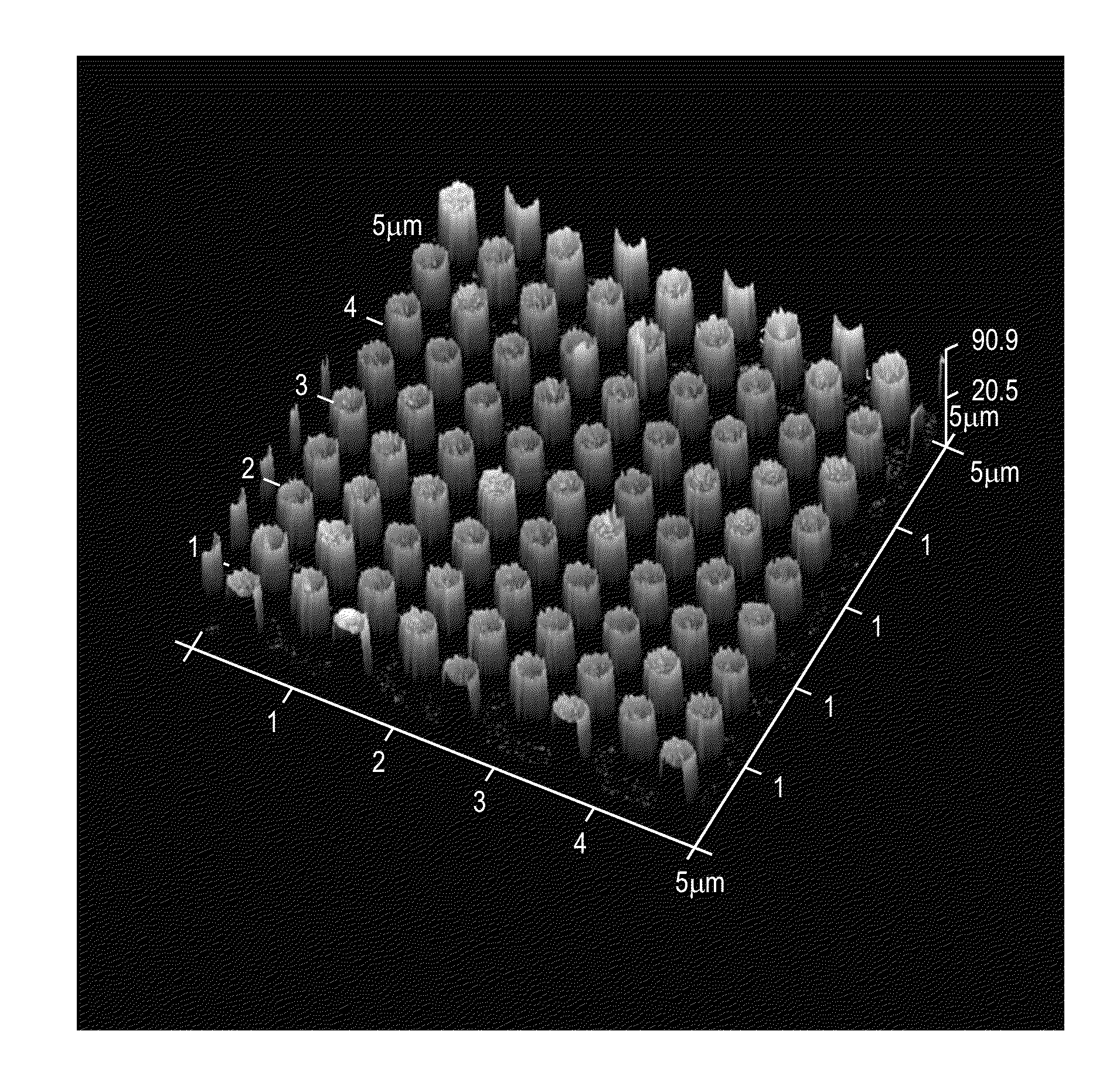
[0126]Formation of contact hole patterns. A solution comprising a 193 nm photoresist (JSR2073) was spin-coated onto a substrate having an anti-reflection layer coating (780 angstroms of ARC29A, Brewer Science) on silicon. The photoresist layer was baked at 110° C. for 60 seconds, patternwise exposed using 193 nm optical lithography, and post exposure baked at 110° C. for 60 seconds. This was followed by a 30 second puddle development step with 0.26 N TMAH developer to resolve 0.25 micrometer contact hole features.


PUM

PropertyMeasurementUnit
circular diameteraaaaaaaaaa
wavelengthaaaaaaaaaa

Abstract

A method of preparing particles comprises forming by optical lithography a topographic template layer disposed on a surface of a substrate, which is suitable for spin casting. The template layer comprises a non-crosslinked template polymer having a pattern of independent wells therein for molding independent particles. Spin casting a particle-forming composition onto the template layer forms a composite layer comprising the template polymer and the particles disposed in the wells. The composite layer is removed from the substrate using a stripping agent that dissolves the template polymer without dissolving the particles. The particles are then isolated.

Description

BACKGROUND[0001]The invention relates to methods of forming nanoparticles using semiconductor manufacturing infrastructure, and more specifically to fabrication of particles having a defined shape and size using lithographically defined templates to mold the nanoparticles.[0002]Nanoparticles have received significant interest for both diagnostic and therapeutic medical applications. Nanoparticles are particularly well suited for drug delivery applications. Many therapeutic agents, including drug molecules, siRNA, and proteins, have a short half-life and are quickly degraded or removed from circulation within the body. Other drug candidates exhibit poor solubility characteristics. Nanoparticles can serve as delivery vehicles, thereby mitigating the challenges of drug delivery and enhancing therapeutic activity by extending drug half-life, improving drug solubility, reducing immunogenicity, and controlling drug release (Shi, J.; Votruba, A. R.; Farokhzad, O. C.; Langer, R. NanoLett. 2...

Claims


Application Information

Patent Timeline
Patent Type & Authority Patents(United States)
IPC IPC(8): B81C1/00B29B9/16B82Y40/00
CPCB29B9/16B81C1/00214B82Y40/00
Inventor CHENG, JOYCOADY, DANIEL J.COLBURN, MATTHEW E.DAVIS, BLAKE W.HEDRICK, JAMES L.HOLMES, STEVEN J.MAUNE, HAREEM T.NELSON, ALSHAKIM
Owner IBM CORP
Why Eureka
Try Eureka