N-type aluminum nitride single-crystal substrate and vertical nitride semiconductor device
a technology of aluminum nitride and single crystal substrate, which is applied in the direction of crystal growth process, polycrystalline material growth, chemically reactive gas growth, etc., can solve the problems of difficult to produce single crystal layer with high crystalline quality, and the conventional art has not yet realized the vertical semiconductor device. , to achieve the effect of high withstand voltage characteristi
- Summary
- Abstract
- Description
- Claims
- Application Information
AI Technical Summary
Benefits of technology
Problems solved by technology
Method used
Image
Examples
example 1
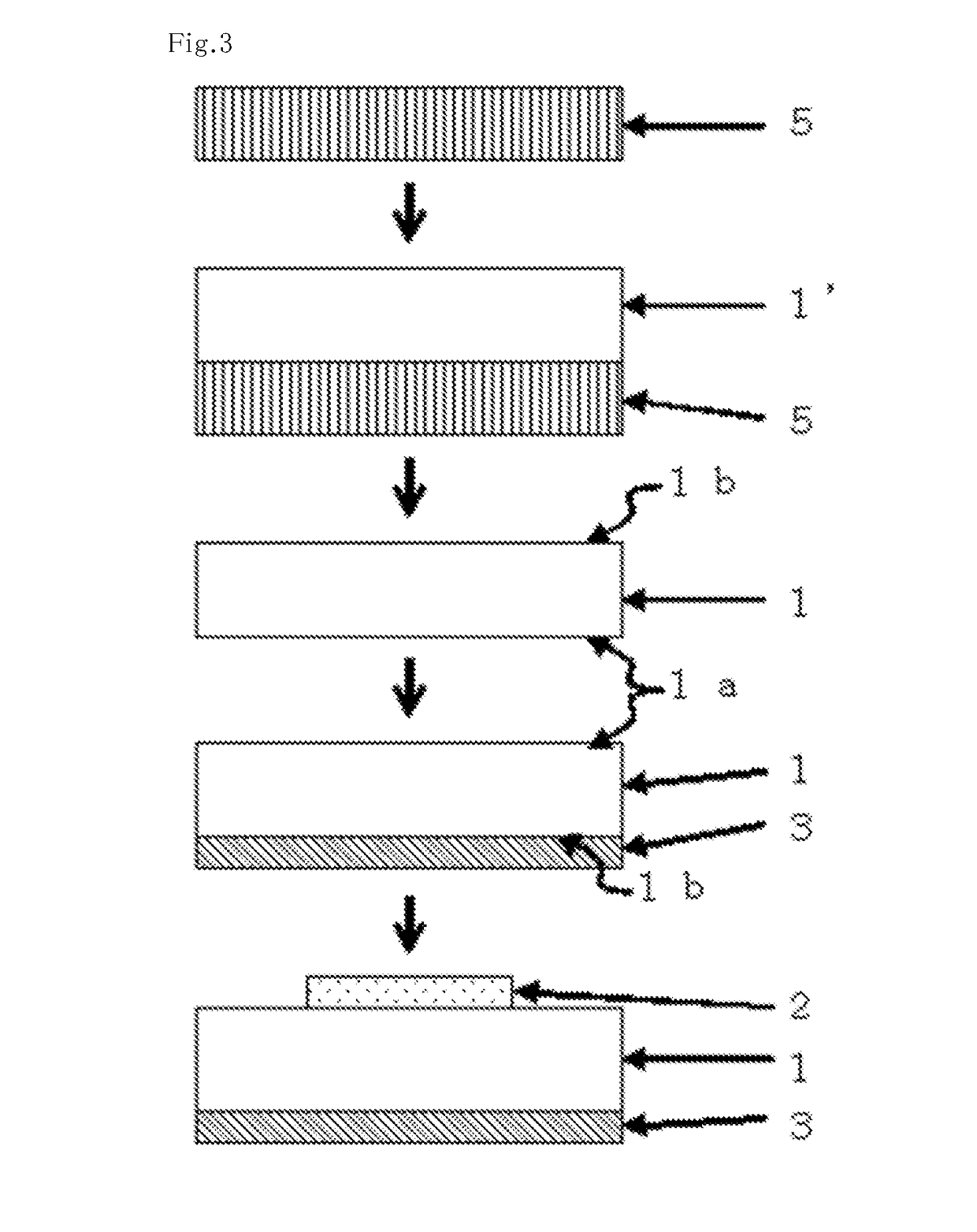
[0096]For the aluminum nitride single crystal seed substrate for producing the n-type aluminum nitride single crystal substrate of the present invention, C-plane aluminum nitride single crystal seed substrate (□15 mm×thickness 500 μm) was used. The dislocation density (the etch pit density) of this aluminum nitride single crystal seed substrate was 1×104 cm−2. Note that, this dislocation density was obtained by the same method as the measuring method of the dislocation density of the n-type aluminum nitride single crystal substrate as described in the following.
[0097]After this seed substrate was placed on the susceptor made of pyrolytic boron nitride of the HVPE reactor, the pressure in the HVPE reactor was set to 750 Torr, then the seed substrate was heated to 1450° C. under the mixed carrier gas of hydrogen and nitrogen atmosphere. Here, the ammonia gas was supplied so that it satisfies 0.5 vol % with respect to the entire carrier gas flow amount (10 slm). Next, the aluminum chlo...
example 2
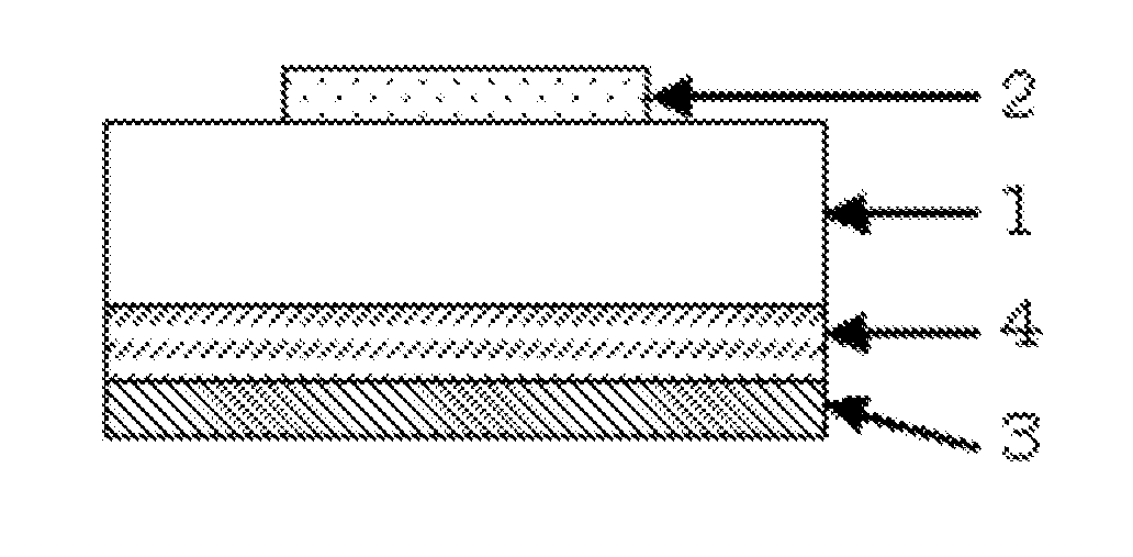
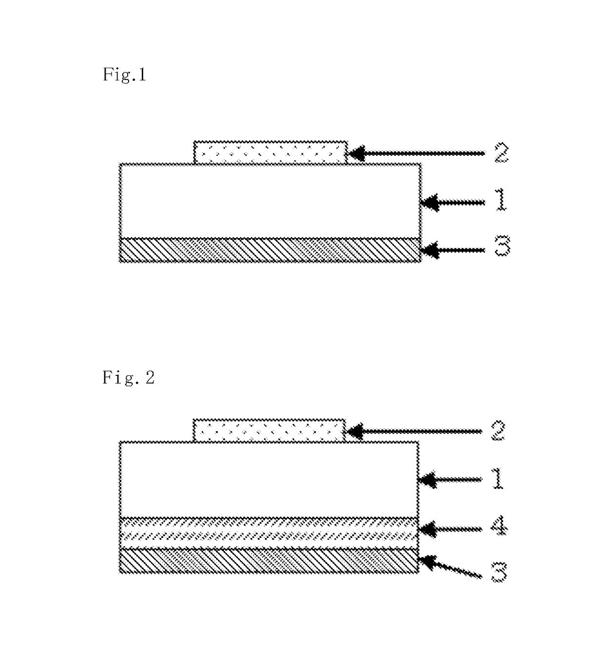
[0104]The vertical Schottky barrier diode was produced and the evaluation was carried out as same as the example 1 by using one of other substrates of which the surface was washed in the hydrochloric acid heated to 40° C. in the example 1; except that the ohmic electrode layer was formed on the N polarity plane side and the Schottky electrode layer was formed on the Al polarity plane. The electrical current—electrical voltage characteristic is shown in FIG. 6. The Schottky diode characteristic with turn on voltage of 10 V or so was obtained. Also, as similar to the example 1, the electrical current was 5×10⁻⁷ Acm−2 when the reverse voltage was 100 V.
example 3
[0105]The vertical Schottky barrier diode was produced and the evaluation was carried out as same as the example 1 by using one of other substrates of which the surface was washed in the hydrochloric acid heated to 40° C. in the example 1; except that 30 nm thick n-type Al0.7Ga0.3N layer was grown on the Al polarity plane side of the substrate by MOVPE at 1080° C., and the ohmic electrode layer was formed at the Al polarity plane side of the n-type Al0.7Ga0.3N layer and the Schottky electrode layer was formed at the N-polarity plane side of the substrate. Note that, Si concentration in n-type Al0.7Ga0.3N layer measured by SIMS analysis was 1×1019 cm−3. The electrical current—electrical voltage characteristic is shown in FIG. 6. The Schottky barrier diode characteristic with turn on voltage of 3 V or so was obtained. Also, as similar to the example 1, the electrical current was 5×10⁻⁷ Acm−2 when the reverse voltage was 100 V.
PUM
 Abstract
Description
Claims
Application Information


