Semiconductor and other materials by thermal neutron transmutation

a technology of semiconductors and other materials, applied in the field of semiconductor device manufacturing, can solve the problems of high cost of photovoltaic modules, and high cost of silicon wafer starting silicon wafers

Inactive Publication Date: 2018-02-06
FULLER MICHAEL KEITH
View PDF16 Cites 5 Cited by
  • Summary
  • Abstract
  • Description
  • Claims
  • Application Information

AI Technical Summary

Benefits of technology

[0013]It is an aim of the present invention to provide a low-cost yet reliable method for fabricating multiple p-n junctions in semiconductor material, in that small dimensions of such junctions are maintained, and associated lattice dislocations of such junctions may be preferentially maintained, and unique electronic devices with such fabricated multiple p-n junctions. Typically, such semiconductor is a silicon wafer and the desired p-n junctions are vertical, continuous between both major surfaces of the wafer, presuming such wafer is oriented horizontally. The method can be described as patterned neutron transmutation doping using neutron optics. The invention is somewhat analogous to ultraviolet light projection microlithography, commonly used to form small patterns in photoresist in the manufacture of integrated circuits. This aim is achieved in the present invention by a method for obtaining patterned p-n junctions in semiconductor material, comprising:
[0021]In a preferred embodiment of the present invention, a manufacturing apparatus for generating fine pattern(s) of thermal neutron exposure, includes an exit surface of a neutron moderating material as a source of thermal neutrons, a periodic one-dimensional (1-D) absorption mask for spatially modulating transmitted neutron intensity, and in the same orientation as the mask / grid, an array of focusing optics, such as an array of compound refractive neutron lenses, that capture and focus such transmitted neutrons such that a striped pattern is projected to semiconductor material, with such pattern possibly being de-magnified in relation to the size of the absorption mask. Stepping the position of the semiconductor material would allow for a complete exposure. Re-orientation of the semiconductor material would allow for complex patterns.
[0031]By introducing a strain field created by local distortions on an atomic scale in the structure of a semiconducting or insulating crystal, it is possible locally to modify the properties of the associated bandgap. One consequence of this is that it has proved feasible to fabricate radiation-emitting devices from materials such as silicon.
[0034]According to this invention, a photovoltaic cell can be made having a body portion of a depletable multiple-region (multiple p-n junctions) semiconductor material that comprises alternating p-type and n-type doped regions extend through the full body. The regions together provide a voltage-sustaining space-charge zone when depleted in a blocking state of the semiconductor. Typically, the p-type silicon body is exposed to neutron irradiation in accordance with this invention such that certain regions, have many silicon atoms transmuted to phosphorus atoms thereby, become n-typed doped regions. At each junction, a depletion zone is formed. Photons arriving at various depths in these depletion zones are highly likely to be converted to electron-hole pairs. Function is improved by including an insulating / reflective coating and an anti-reflection coating. Backside interlaced metal traces provide a means of moving charge.

Problems solved by technology

The photovoltaic solar cell industry is extremely cost sensitive, and the cost of a starting silicon wafer is typically nearly half of the value of the finished photovoltaic module.
High-purity silicon crystal offsets some of these losses by providing an extended diffusion length, but is more expensive to produce and still has deep regions that poorly contribute to electron-hole pair conversion.
Depth of light conversion is also strongly related to photon energy (wavelength), resulting in losses of otherwise useful parts of the solar spectrum.
Two problems exist for Grover's method; one, thermal neutrons are not easily collimated, and two, masks have large feature sizes as a result of their manufacturing methods.
Similar limitations occur in the exposure step in x-ray proximity lithography, which has most of the same elements as described in Grover's method.
The standard approach for collimating x-rays used at synchrotron facilities, which is to provide great distance from a small origin to the work necessary for proximity lithography, is not effective for thermal neutrons.
Additionally, thermal neutrons are relatively slow moving, heavy particles with flight paths that are affected by gravity.
Unfortunately, most photons are absorbed in regions that are shallower or deeper than the depletion zone and overall light-to-electricity efficiency is reduced.
Silicon, on the other hand, has been considered fundamentally unsuitable for use as an emitter of radiation.
With the continuing and rapid development of computer processors, the constant demand for increased processing power and speed and reduced size necessitates an ever increasing complexity of the interconnecting metallisations.
It is anticipated that this complexity will eventually present an insurmountable obstacle to further development (the breakdown of Moore's Law) because electrons will spend a disproportionate amount of time in the metallisations instead of in the components they interconnect, thereby curtailing processing power and speed.
Some attempts of ion implantation to form strain fields within silicon have had limited success, with poor focusing at higher energy / penetration depths being the main drawback (Homewood et al, U.S. Pat. No. 7,274,041).

Method used


Image

  • Semiconductor and other materials by thermal neutron transmutation
  • Semiconductor and other materials by thermal neutron transmutation
  • Semiconductor and other materials by thermal neutron transmutation

Examples


Embodiment Construction

General Aspects

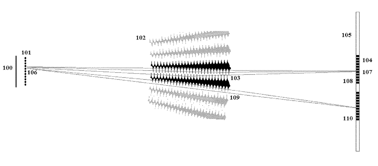
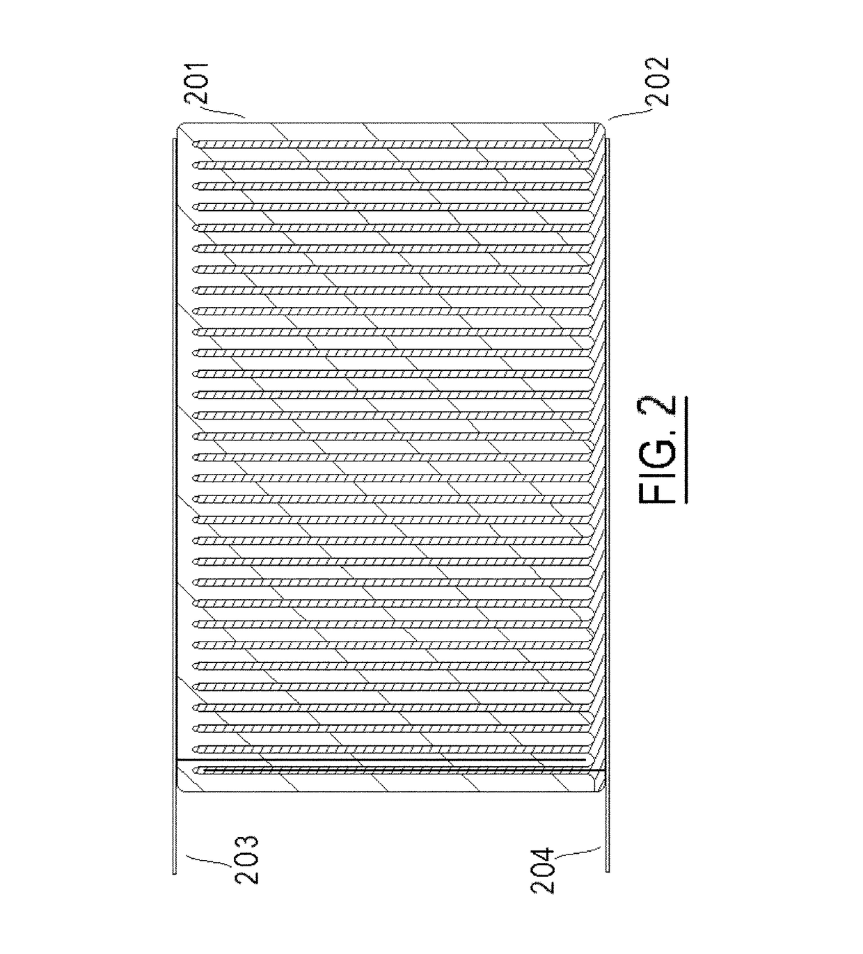
[0043]FIG. 1, is a schematic diagram of a manufacturing apparatus according to one embodiment of the disclosed invention, shown in the “side view,” having an exit surface of a neutron moderating material 100 as a source of thermal neutrons, a primary periodic one-dimensional (1-D) absorption mask 101 for spatially modulating transmitted intensity, and in the same orientation as the mask / grid, an array of focusing optics 102, such as an array of compound refractive neutron lenses. Portions of the primary mask-modulated field of thermal neutron-radiation are captured and focused by an individual optic 103 in the array 102 such that a striped pattern 104 is formed at the semiconductor material 105. As shown, the lens array consists of extruded ribbons of low-Z material with each major surface of each ribbon sculpted as to form a half-lens. Again as shown, the diameter of individual lens elements increases in size from one edge of the ribbon to the other. When assembled p...


PUM

PropertyMeasurementUnit
elemental compositionaaaaaaaaaa
doping concentrationaaaaaaaaaa
thicknessaaaaaaaaaa

Abstract

A method of manufacturing p-n junction in semiconductor material such that small dimensions of such junctions are maintained, and associated lattice dislocations of such junctions may be preferentially maintained, and devices with such patterned semiconductor material, is disclosed. Typically, a neutron moderator is used to slow fast neutrons to thermal energies. A mask made from thermal neutron absorbing material, such as cadmium, is placed in close proximity to such neutron moderator. Thermal neutron focusing optics, such as compound refractive lenses, are used to collect and focus thermal neutrons emitted from the mask such that the pattern or portion of the pattern is transferred to the silicon body, with neutrons transmitted from the window areas in the mask and through the neutron optic so as to form the donor dopant concentration for the n-type regions by transmutation of silicon atoms into phosphorus. An electronic device produced by such a method has vertical p-n junctions continuous between both major surfaces and horizontal alternating p-type and n-type regions across most of the face of the material, such that unique properties are achieved.

Description

BACKGROUND OF THE INVENTION[0001]This invention relates to the manufacture of semiconductor devices with a depletable multiple-region semiconductor material that provides a voltage-sustaining space-charge zone when depleted, and to a method of fabricating such a material. The invention also relates to other semiconductor material and semiconductor devices produced by such methods.[0002]The voltage-sustaining space-charge zone results from charge-carrier depletion of interposed p-type and n-type regions that form multiple p-n junctions in the material. The intermediate dimensions (width or thickness) of the interposed p-type and n-type regions need to be small enough (in relation to their dopant concentrations) to allow depletion of the region across its intermediate dimension without the resulting electric field reaching the critical field strength at which avalanche breakdown would occur in that semiconductor. This is an extension of the famous RESURF principle. Thus, the depletabl...

Claims


Application Information

Patent Timeline
Patent Type & Authority Patents(United States)
IPC IPC(8): H01L21/26H01L31/18H01L31/0288H01L35/34H01L35/22H01L29/167H01L29/06H01L29/66H01L21/78H01L21/18H01S5/32H01L21/66H01L31/0216H01L21/261H01L33/00H01L33/34
CPCH01L21/261H01L33/0054H01L33/343H01L31/1804H01L31/0288H01L35/34H01L35/22H01L29/167H01L29/063H01L29/66568H01L21/78H01L21/187H01S5/3224H01L22/12H01L31/02168H01L29/7802H01L29/0634H01L33/24H01L31/0475Y02E10/547Y02P70/50H10N10/855H10N10/01
Inventor FULLER, MICHAEL KEITH
Owner FULLER MICHAEL KEITH
Why Eureka
Try Eureka