Mixed technology integrated device comprising complementary LDMOS power transistors, CMOS and vertical PNP integrated structures having an enhanced ability to withstand a relatively high supply voltage

Inactive Publication Date: 2001-10-30
STMICROELECTRONICS SRL
14 Cites 35 Cited by

AI-Extracted Technical Summary

Problems solved by technology

This makes difficult interfacing the power transistor (e.g. VDMOS) with the driving circuitry.
In "smart power" type integrated circuits, th...

Method used

...

Benefits of technology

The CMOS structures formed by pairs of complementary LDMOS transistors, when provided with such an n-doped region by phosphorus implantation, become capable of operating with a supply voltage of about 20 V without requiring special precautions, such as "field plates", thus remaining advantageously compact.
In the case of an n-channel MOS transistor belonging to another type of CMOS structure, the n-doped region, obtained by phosphorus implantation in the drain area of the transistor, reduces the sensitivity to electrical stresses due to hot electrons, by acting as a "drain extension" region; this permits to the transistor to withstand a supply voltage of about 12 V.
In the case of an isolated collector, vertical PNP bipolar transistor, the additional n-doped r...

Abstract

Complementary LDMOS and MOS structures and vertical PNP transistors capable of withstanding a relatively high voltage may be realized in a mixed-technology integrated circuit of the so-called "smart power" type, by forming a phosphorus doped n-region of a similar diffusion profile, respectively in: The drain zone of the n-channel LDMOS transistors, in the body zone of the p-channel LDMOS transistors forming first CMOS structures; in the drain zone of n-channel MOS transistors belonging to second CMOS structures and in a base region near the emitter region of isolated collector, vertical PNP transistors, thus simultaneously achieving the result of increasing the voltage withstanding ability of all these monolithically integrated structures. The complementary LDMOS structures may be used either as power structures having a reduced conduction resistance or may be used for realizing CMOS stages capable of operating at a relatively high voltage (of about 20V) thus permitting a direct interfacing with VDMOS power devices without requiring any "level shifting" stages. The whole integrated circuit has less interfacing problems and improved electrical and reliability characteristics.

Application Domain

Technology Topic

Image

  • Mixed technology integrated device comprising complementary LDMOS power transistors, CMOS and vertical PNP integrated structures having an enhanced ability to withstand a relatively high supply voltage
  • Mixed technology integrated device comprising complementary LDMOS power transistors, CMOS and vertical PNP integrated structures having an enhanced ability to withstand a relatively high supply voltage
  • Mixed technology integrated device comprising complementary LDMOS power transistors, CMOS and vertical PNP integrated structures having an enhanced ability to withstand a relatively high supply voltage

Examples

  • Experimental program(1)

Example

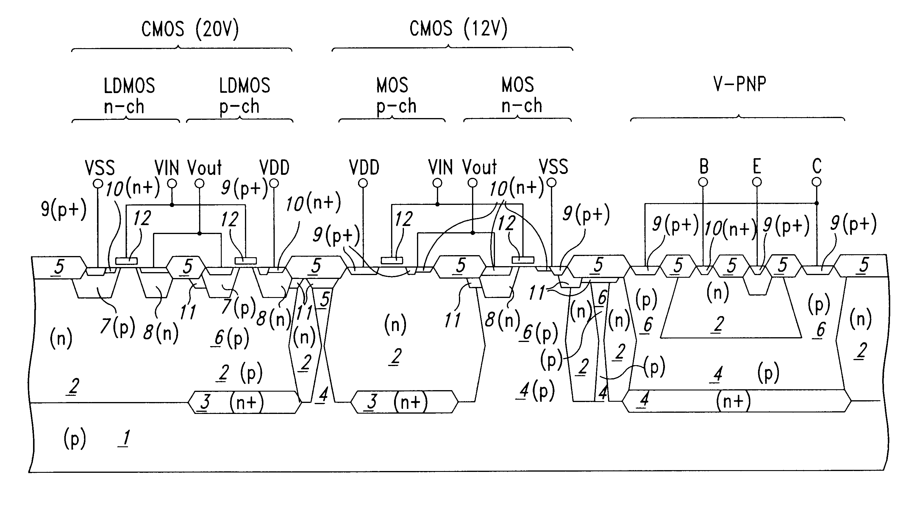
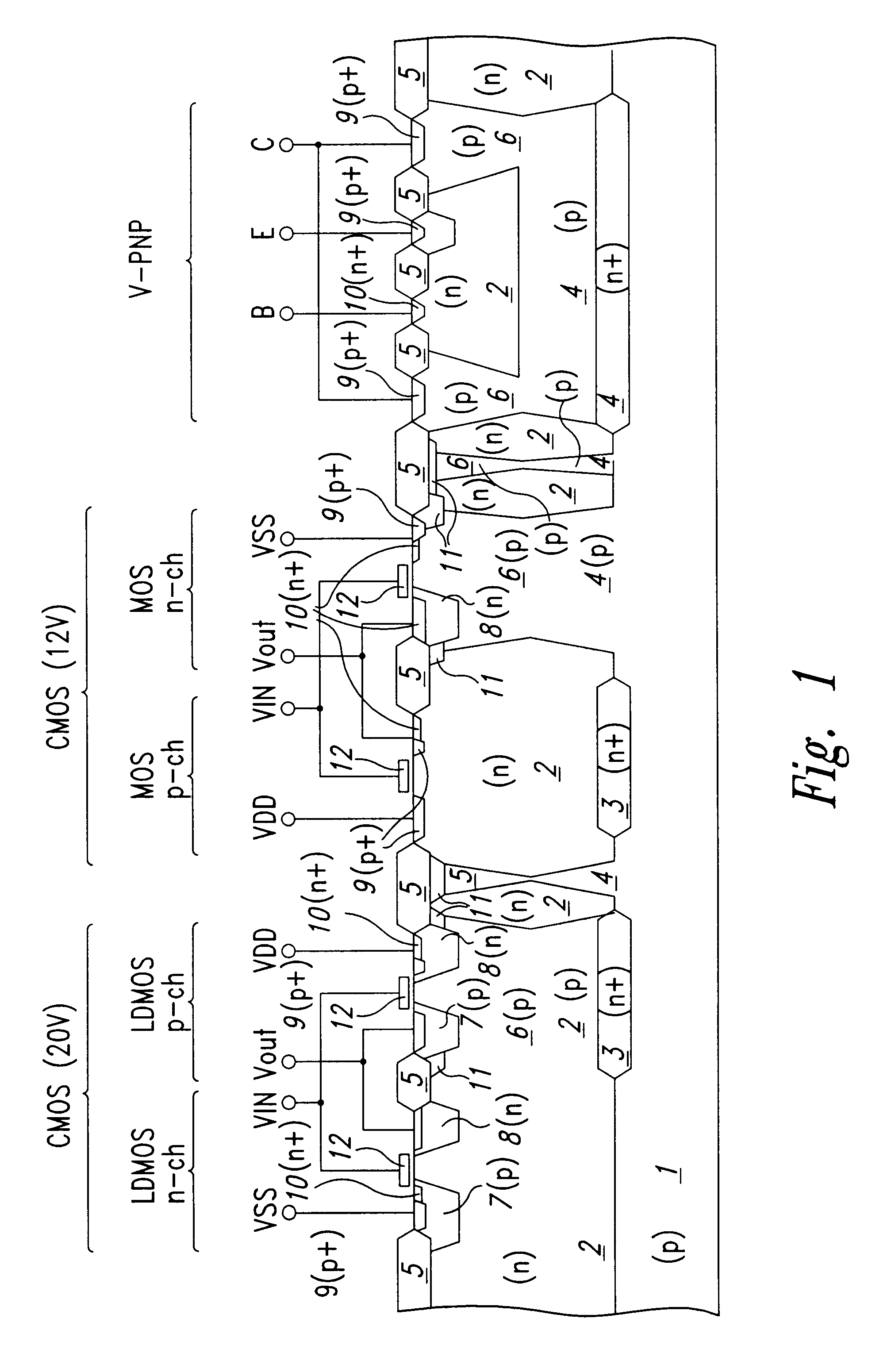
An hypothetical partial cross section of an integrated "smart power" type integrated device, wherein it is relatively easy to put in evidence, though in a schematic way, the aspects of the invention, is shown in FIG. 1. The depicted cross section does not include VDMOS power transistors, which may be easily imagined present in a different zone of the integrated device from the zone shown in the partial cross section of the figure, wherein two different CMOS structures are depicted, a first structure formed by an n-channel and a p-channel LDMOS transistor and a second structure formed by a p-channel and by an n-channel MOS transistor, and the structure of an isolated collector, vertical PNP bipolar transistor.
The device comprises a p-type silicon substrate 1 on which an epitaxial n-type silicon layer 2 has been grown after doping with arsenic and/or with boron certain areas defined on the surface of the monocrystalline silicon substrate 1 in order to form the n.sup.+ buried layers 3 and the p-type bottom isolations 4. The integrated device further comprises an isolation structure among the different integrated devices which, in the depicted example, is formed by a field oxide layer 5 grown on the surface of the silicon 2, after doping with boron .[.predifined.]. .Iadd.predefined .Iaddend.areas on the silicon surface in order to form, in accordance with well known techniques, the p-well regions 6 (i.e. top isolations and p-well) as well as regions with a heavier boron doping charge 11, also known as p-field region, while growing the field oxide 5, according to a known technique.
Within active areas destined to the formation of MOS-type devices, gate structures 12, commonly of doped polycrystalline silicon, are formed.
Typically the n-channel, LDMOS transistor comprises a p-body region 7, produced in the silicon by implanting boron under self-alignment conditions in the source area extending between the gate 12 and the field oxide 5 and by successively diffusing the implanted boron until obtaining the desired diffusion profile of the region 7, the n.sup.+ source and drain junctions 10 and the p.sup.+ region 9 having a relatively high doping level formed in the source region for contacting the body region 7.
Similarly a p-channel LDMOS transistor comprises a p-doped region 7 (having substantially the same profile of the n-channel LDMOS body region), formed in the drain region of the transistor, the p.sup.+ drain and source junctions 9 and the n.sup.+ region 10, formed in the source area in order to contact an n-body region, the formation of which together with other n-regions in the different integrated structures according to the present invention will be described later.
The p-channel MOS transistor forming the second CMOS structure depicted in FIG. 1, comprises, as usual, the source and drain p.sup.+ junctions 9 and a "back gate" contact, n.sup.+ region 10, formed in the source zone of the transistor. Similarly the n-channel MOS transistor comprises the n.sup.+ source and drain junctions 10 and a "back gate" contact, p.sup.+ region 9, formed in the source zone of the transistor.
The structure of the isolated collector PNP vertical transistor comprises the collector (C) and emitter (E) contact p.sup.+ diffusions 9 and the base (B) n.sup.+ contact diffusion 10.
In accordance with the present invention, an n-type region 8, doped with phosphorus, extends from the surface of the epitaxial layer respectively in the drain area of the n-channel LDMOS transistor extending between the gate electrode and the isolation field oxide, in the source area of the p-channel LDMOS transistor extending between the gate electrode and the isolation field oxide, in the drain area of the n-channel MOS transistor extending between the gate electrode and the adjacent isolation field oxide and in the emitter area of the isolated collector PNP bipolar transistor defined by the surrounding isolation field oxide, for a depth sufficient to contain at least, respectively, the n.sup.+ drain junction of the n-channel LDMOS transistor, the p.sup.+ source junctions and n.sup.+ body contact regions of the p-channel LDMOS transistor, the n.sup.+ drain junction of the n-channel MOS transistor and the n.sup.+ emitter junction of the PNP transistor.
These n-type regions 8 are made evident in the schematic cross section depicted in FIG. 1 by means of a thick line.
As it will be evident to the skilled technician, the distinct regions 8 may be easily formed simultaneously in the indicated zones without requiring critical process steps by simply implanting phosphorus under self-alignment conditions in the indicated areas and by diffusing the implanted phosphorus before proceeding to the formation of the heavily doped n.sup.+ regions obtained by implanting arsenic and diffusing it and of the heavily doped p.sup.+ regions obtained by implanting boron and diffusing it, which are contained within said auxiliary regions 8. In a normal fabrication process the doping level of this additional n-region 8 may be comprised between 10.sup.13 and 10.sup.14 (phosphorus) atoms per cubic centimeter.
Shown in FIG. 2 are the equimodal electric field lines in the overlapping region between the drain and the gate of an n-channel LDMOS transistor having a 600 Angstroms (A) thick gate oxide, produced by means of computer model simulation for the case of a transistor without the auxiliary n-doped region (8 of FIG. 1) in accordance with the present invention and subjected to a 20 V bias. The maximum electric field intensity is evaluated to be 6.times.10.sup.5 V/cm.
Similarly, shown in FIG. 3 are the equimodal electric field lines in the same overlapping region under identical bias conditions (20 V) of the example shown in FIG. 2, but wherein the n-channel LDMOS transistor is provided with the auxiliary n-region, doped with phosphorus at 10.sup.14 atoms per cubic centimeter, in accordance with the present invention. As it is easily noted by comparing the FIGS. 2 and 3, in the latter the equimodal electric field lines are more "distended" than those of FIG. 1 and the maximum field electric intensity may be evaluated to be 5.times.10.sup.5 V/cm. This is 17% less than the maximum intensity evaluated in the case of the transistor of the prior art without the .[.auxialiary.]. .Iadd.auxiliary .Iaddend.phosphorus doped region.
The CMOS structure formed by the complementary LDMOS transistors provided with the n-doped region 8 (FIG. 1) in accordance with the present invention may .[.funtions.]. .Iadd.functions .Iaddend.with a supply voltage of 20 V and it may be directly interfaced, as a driving device, with VDMOS power transistors for example, thus eliminating the need for adequate level shifting circuits. Moreover, an LDMOS transistor structure modified according to the invention is intrinsically capable of withstanding voltages in the order of 20 V without requiring the formation of "field plates" (according to a known technique for increasing the intrinsic breakdown voltage of integrated transistors) which inevitably clashes with compactness requirements of these integrated structures.
Naturally, as it will appear evident to the skilled technician, the complementary LDMOS transistors, depicted as forming a CMOS structure in FIG. 1, may themselves be employed as power transistors through an appropriate layout configuration, exploiting also for such applications, the same improved performance in terms of voltage withstanding ability and reduced resistance (R.sub.on), derived by the presence of said additional n-region 8, in accordance with the present invention.
Also the electrical performances of the other CMOS structure shown, formed by the pair of complementary MOS transistors, are improved because the n-region 8 formed in the drain region of the n-channel transistor acts as a drain extension region thus increasing the nominal operating voltage of the relative CMOS structure.
Another, .[.non-negligeable.]. advantage is obtained also in terms of improved performance of the isolated collector, vertical PNP bipolar transistor by providing also this integrated device with the n-region 8 doped with phosphorus .[.enchroaching.]. .Iadd.encroaching .Iaddend.in the base region of the transistor. The consequent increase of the doping level of the base region reduces sensitivity to depletion of the base region thus increasing the punchthrough voltage between emitter and collector. This permits also to this integrated component of the "smart power" device to function under a relatively high voltage, thus broadening the possibility of employing this type of transistor which is outstandingly suited, in respect to other types of transistors, for implementing circuits with a higher cut-off frequency then that which may be obtained by means of lateral PNP transistors.

PUM

no PUM

Description & Claims & Application Information

We can also present the details of the Description, Claims and Application information to help users get a comprehensive understanding of the technical details of the patent, such as background art, summary of invention, brief description of drawings, description of embodiments, and other original content. On the other hand, users can also determine the specific scope of protection of the technology through the list of claims; as well as understand the changes in the life cycle of the technology with the presentation of the patent timeline. Login to view more.

Similar technology patents

Field effect transistor

InactiveUS20100224870A1Good environmental stabilityReduce sensitivityTransistorVacuum evaporation coatingPhysicsAmorphous oxide
Owner:CANON KK

Crosslinkable acrylate adhesive polymer composition

InactiveUS20110178248A1Reduce sensitivityHigh shear strengthEster polymer adhesivesSolventPolyaziridine
Owner:3M INNOVATIVE PROPERTIES CO

Classification and recommendation of technical efficacy words

  • Improve performance
  • Reduce sensitivity

Electrical muscle controller

Owner:IMPULSE DYNAMICS NV
Why Eureka
Try Eureka