Highly heat-resistant synthetic polymer compound and high withstand voltage semiconductor device

A technology for synthesizing polymers and compounds, which is applied in semiconductor devices, semiconductor/solid-state device parts, electric solid-state devices, etc. The effect of high dispersion effect

Inactive Publication Date: 2008-01-16
THE KANSAI ELECTRIC POWER CO +1
View PDF2 Cites 3 Cited by
  • Summary
  • Abstract
  • Description
  • Claims
  • Application Information

AI Technical Summary

Problems solved by technology

That is, the creeping distance between the exposed side 90a not covered by the passivation film 98 and the anode electrode 96 is short, so the reverse breakdown voltage cannot be increased.

Method used


Image

  • Highly heat-resistant synthetic polymer compound and high withstand voltage semiconductor device
  • Highly heat-resistant synthetic polymer compound and high withstand voltage semiconductor device
  • Highly heat-resistant synthetic polymer compound and high withstand voltage semiconductor device

Examples


no. 1 Embodiment

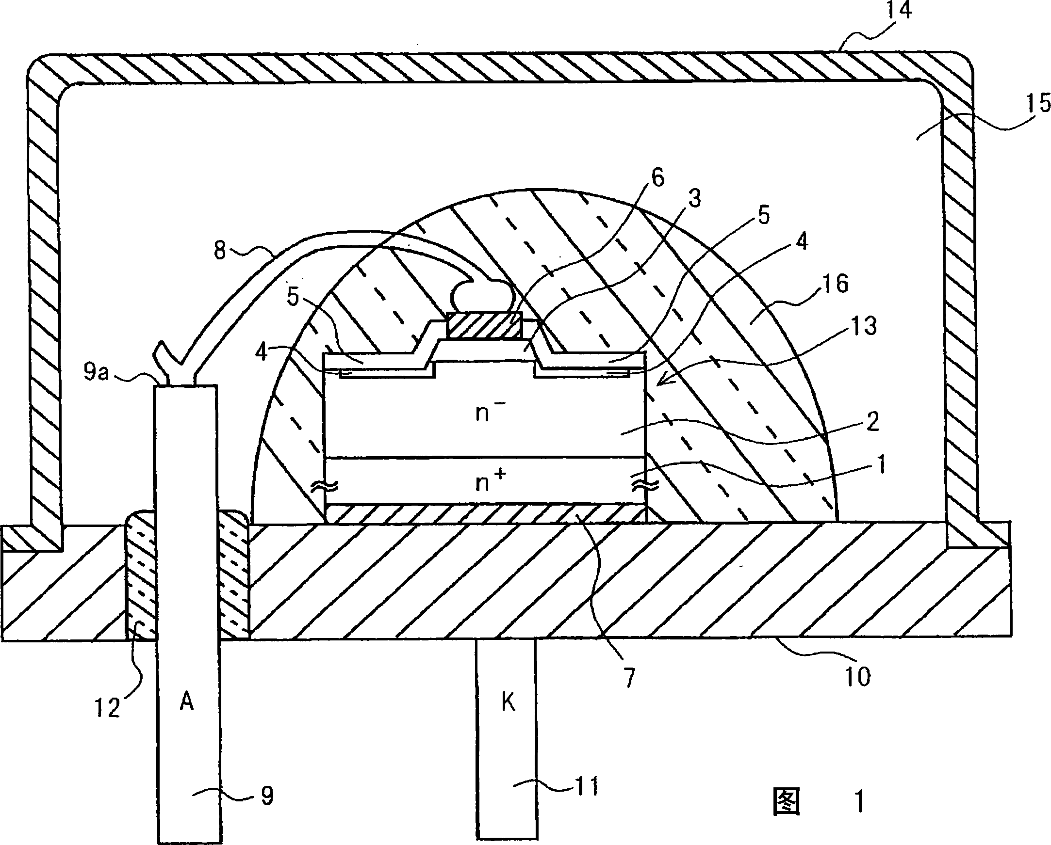
[0072] 1 is a cross-sectional view of a high heat-resistant and high-voltage semiconductor device according to a first embodiment of the present invention. In the semiconductor device of this embodiment, a high withstand voltage SiC (silicon carbide) pn diode element 13 with a withstand voltage of 8 kV is housed in a case 14, and is composed of a synthetic polymer compound of the present invention with high heat resistance and high heat dissipation. Cover 16 covers SiCpn diode element 13 .

[0073] SiCpn diode element 13 has the following structure. An offset layer 2 of n-type SiC having a thickness of about 90 μm and having a low impurity concentration is formed on the cathode region 1 of n-type SiC having a thickness of about 300 μm and having a high impurity concentration. A cathode electrode 7 is formed below the cathode region 1 . An anode region 3 of p-type SiC forming a main junction is formed in the central region of the offset layer 2 . A metal anode electrode 6 is...

no. 2 Embodiment

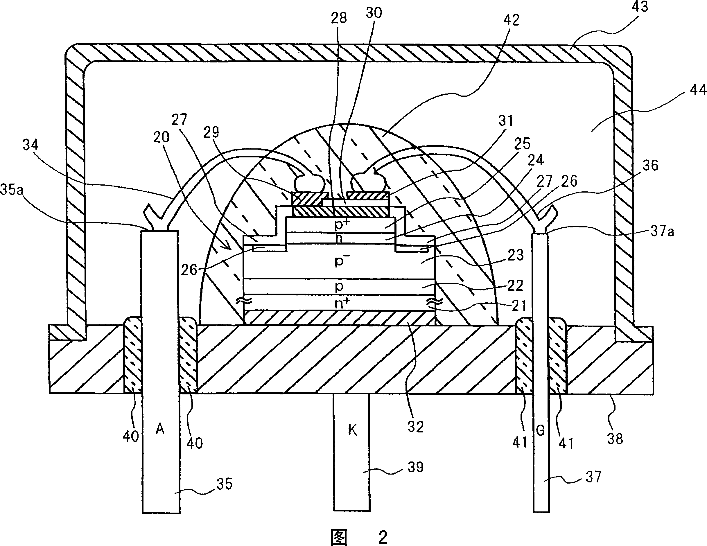
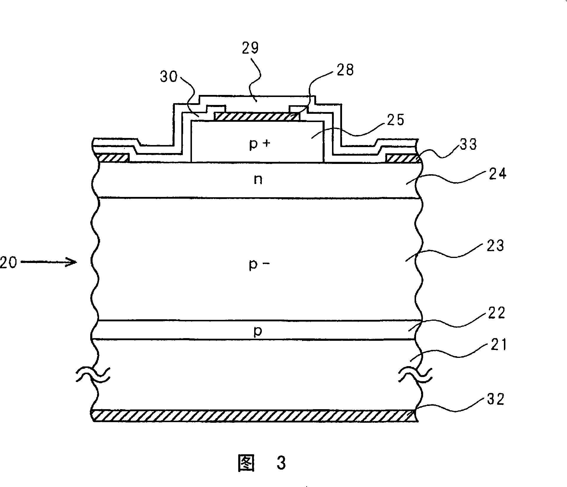
[0085] The semiconductor device according to the second embodiment of the present invention is a SiC-GTO thyristor (Gate Turn off Thyristor) device with a withstand voltage of 5 kV. Fig. 2 is its sectional view. FIG. 3 is a cross-sectional view illustrating a cell formed by cutting the GTO thyristor element 20 in FIG. 2 along a plane perpendicular to the paper. In an actual device, a plurality of units shown in FIG. 3 are connected in the left and right directions of the figure. In FIGS. 2 and 3 , a buffer layer 22 of p-type SiC having a thickness of about 3 μm is provided on the cathode region 21 of n-type SiC having a thickness of about 320 μm and a high impurity concentration. A cathode electrode 32 is arranged below the cathode region 21 . An offset layer 23 of p-type SiC with a low impurity concentration of approximately 60 μm in thickness is provided on buffer layer 22 . An n-type base region 24 and a p-type anode region 25 having a thickness of approximately 2 μm are...

no. 3 Embodiment

[0101] An optically coupled wide-gap power semiconductor device, which is a semiconductor device according to a third embodiment of the present invention, will be described with reference to the cross-sectional view of FIG. 4 . In this embodiment, a GaN (gallium nitride)-npn bipolar (type) transistor 51 with a withstand voltage of 3 kV / current capacity of 200 A is used as a power semiconductor element having a light emitting function. A SiC-photodiode 52 is used as a light receiving element. The SiC photodiode 52 is disposed in the same housing as the GaN-npn bipolar (type) transistor 51 .

[0102]In the GaN-npn bipolar (type) transistor 51 shown in FIG. 4 , a p-type GaN base region 54 with a thickness of about 1.7 μm is formed on an n-type GaN collector region 53 with a thickness of about 300 μm and a high impurity concentration, An n-type emitter region 55 having a thickness of about 3 μm and a high impurity concentration is formed thereon. A collector electrode 66 is prov...


PUM

PropertyMeasurementUnit
electric potential / voltageaaaaaaaaaa
glass transition temperatureaaaaaaaaaa

Abstract

The outer surface of a wide-gap semiconductor device is covered with a synthetic polymer compound. The synthetic polymer compound is formed by linking a plurality of third organosilicon polymers through covalent bonding which is formed by addition reaction, and has a three-dimensional steric structure. The third organosilicon polymers are obtained by linking one or more kinds of first organosilicon polymers having a bridge structure formed by siloxane bonds (Si-O-Si bonds) with one or more kinds of second organosilicon polymers having a linear structure formed by siloxane bonds. Insulating ceramic fine particles having high heat conductivity are preferably mixed with the synthetic polymer compound.

Description

technical field [0001] The present invention relates to a synthetic high molecular compound with high heat resistance and a high withstand voltage power semiconductor device covered with the synthetic high molecular compound. The semiconductor device has high heat resistance and good heat dissipation. Background technique [0002] For a power semiconductor device that handles relatively large power, the temperature of the semiconductor device becomes high due to heat generated when high-power energization is performed, and such a power semiconductor device is required to have high heat resistance. Power semiconductor devices at the present stage are basically silicon (Si) power semiconductor devices, but the heat resistance limit temperature of Si power semiconductor devices is usually 150°C. Attempts are currently being made to increase the heat-resistant limit temperature of silicon power semiconductor devices to around 200°C. [0003] On the other hand, attempts have bee...

Claims


Application Information

Patent Timeline
Patent Type & Authority Applications(China)
IPC IPC(8): C08G77/44C08L83/10H01L23/29H01L23/31H01L29/744H01L29/861H01L31/12H01L33/00C08K3/14C08K3/22C08K3/28C08L83/04H01L29/868
CPCC08G77/04H01L23/3121H01L2224/73265H01L2924/12044H01L2224/48137H01L2224/32245H01L23/3135H01L2224/48091H01L25/167H01L2924/13063H01L2924/01004H01L23/04H01L23/045H01L2924/01078H01L2924/13055H01L24/48H01L25/072H01L25/074H01L2924/01079H01L2224/45015H01L2224/4823H01L23/24H01L24/45H01L2924/01057H01L2224/45144H01L2924/13091H01L33/56H01L2224/04042H01L2924/16152C08G77/44H01L2224/48465H01L31/0203H01L2924/1301H01L2924/13034H01L2924/12032H01L2924/1305H01L2924/13062H01L2224/8592H01L2224/49107H01L2924/12036H01L2924/12043H01L24/49H01L2924/00014H01L2924/20758H01L2924/00C08G77/42C08L83/04C08K3/14H01L23/29
Inventor 菅原良孝东海林义和
Owner THE KANSAI ELECTRIC POWER CO
Why Eureka
Try Eureka