Nickel plating method for surface of silicon nanowires
A technology of silicon nanowires and nickel plating, which is applied in the field of semiconductor microelectronics and nanoelectronics, can solve the problems of interface electromigration size effect, which cannot meet the shrinkage of device size, etc., and achieve the reduction of resistivity, contact resistance and performance and good structure
- Summary
- Abstract
- Description
- Claims
- Application Information
AI Technical Summary
Problems solved by technology
Method used
Image

Examples
Embodiment 1
[0021] (1) Preparation of silicon nanowires by thermal evaporation of SiO
[0022] The experimental device is a low-vacuum tube furnace (Hefei Kejing, GSL-1400X vacuum tube furnace), which consists of a tube-type heating furnace with a length of 75cm, a corundum tube with a diameter of 60cm and a length of 120cm, a bipolar vacuum pump, and a gas flowmeter. , the vacuum degree of the device can reach 10 -2 torr. Before the experiment, the quartz boat was cleaned with acetone and alcohol, rinsed with deionized water, dried, and then pushed into the end of the tube furnace. At the same time, the small porcelain boat filled with SiO was pushed into the middle of the tube furnace. Vacuum for 30min, at this time the vacuum degree in the furnace reaches 10 -2 torr, after the tube furnace reached 800°C at a heating rate of 15°C / min, Ar gas (purity: 99.999%) was introduced into the furnace at a flow rate of 60 sccm, and the furnace tube was rapidly heated at a heating rate of 20°C / mi...
Embodiment 2
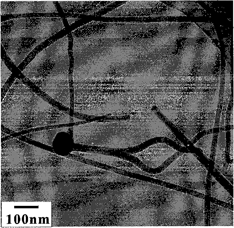
[0030] The preparation and pretreatment of silicon nanowires are the same as in Example 1. The silicon nanowires from which the silicon oxide layer has been removed are ultrasonically dispersed and dropped on a polished silicon wafer. Argon ion sputtering equipment (Denton Discovery-18 sputtering system) is used as the sputtering equipment , the vacuum degree of the sputtering system is 5×10 -6 torr, with 9.1W sputtering power to nickel-plate the surface HF-treated silicon nanowires; set the sputtering time to 240s, the results are as follows image 3 Shown; after sputtering, the surface of silicon nanowires is coated with amorphous nickel particles, on this basis, it is annealed. Annealing is carried out in a tube furnace (Hefei Kejing, GSL-1400X vacuum tube furnace). Before annealing and heating up, a mechanical pump is used to pump the vacuum in the furnace tube to 10 -2 torr, then charge 5×10 4 Pa Ar gas is the protective gas and carrier gas, the Ar flow rate is 300sccm ...
Embodiment 3
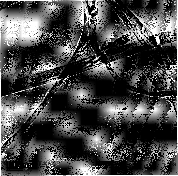
[0032] The preparation and pretreatment of silicon nanowires are the same as in Example 1. The silicon nanowires from which the silicon oxide layer has been removed are ultrasonically dispersed and dropped on a polished silicon wafer. Argon ion sputtering equipment (Denton Discovery-18 sputtering system) is used as the sputtering equipment , the vacuum degree of the sputtering system is 10 -6 torr, with 9.1W sputtering power to nickel-plate the surface HF-treated silicon nanowires; set the sputtering time to 270s, the results are as follows Figure 4 Shown; after sputtering, the surface of silicon nanowires is coated with amorphous nickel particles, on this basis, it is annealed. Annealing is carried out in a tube furnace (Hefei Kejing, GSL-1400X vacuum tube furnace). Before annealing and heating up, a mechanical pump is used to pump the vacuum in the furnace tube to 10 -2 torr, then charge 1×10 5 Pa Ar gas is the protective gas and the carrier gas, the Ar flow rate is 100 s...
PUM
 Abstract
Description
Claims
Application Information
 - Generate Ideas
- Intellectual Property
- Life Sciences
- Materials
- Tech Scout
- Unparalleled Data Quality
- Higher Quality Content
- 60% Fewer Hallucinations
Browse by: Latest US Patents, China's latest patents, Technical Efficacy Thesaurus, Application Domain, Technology Topic, Popular Technical Reports.
© 2025 PatSnap. All rights reserved.Legal|Privacy policy|Modern Slavery Act Transparency Statement|Sitemap|About US| Contact US: help@patsnap.com