Microfine piezoelectric ceramics array structure composite material and preparation thereof
A technology of piezoelectric ceramics and array structure, which is applied in the field of functional ceramic materials and its preparation, can solve problems such as corrosion, and achieve the effects of low annealing temperature, short annealing time, and low requirements
- Summary
- Abstract
- Description
- Claims
- Application Information
AI Technical Summary
Problems solved by technology
Method used
Image
Examples
Embodiment 1
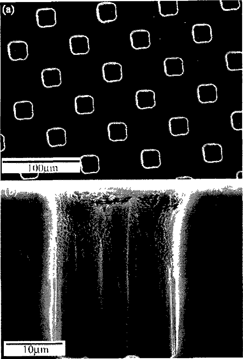
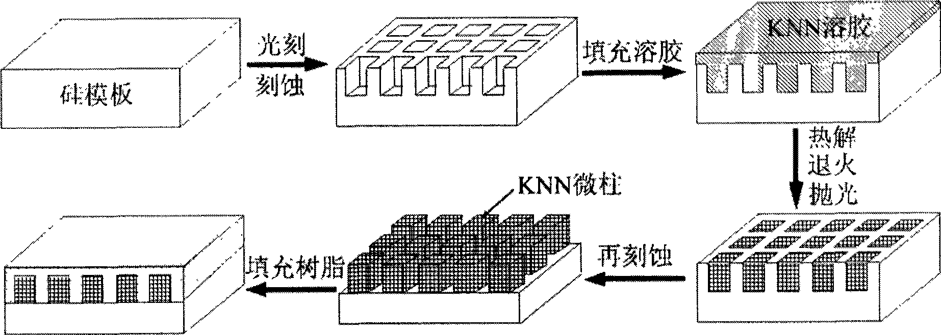
[0035] React K and Na respectively with absolute ethanol to obtain ethanol salt solution, mix and dissolve appropriate amount of potassium ethoxide and sodium ethoxide solution in the ethylene glycol monomethyl ether solvent according to the metal ion ratio of 1:1, add 2mL glacial acetic acid and 2mL Acetylacetone was used as a stabilizer and a chelating agent respectively, and then refluxed and chelated for 4 hours at 120°C in a sol reflux machine, and then pressed K 0.5 Na 0.5 NbO 3 Add niobium ethanol according to the stoichiometric ratio, add 2-3mL ethylene glycol monomethyl ether, glacial acetic acid, acetylacetone, add 1mL formamide, continue to reflux at 120°C for 45min, and finally distill under reduced pressure to reduce the liquid volume to 10mL to obtain 0.3M KNN sol, after cooling, pour it into a weighing bottle and seal it for storage.
[0036] A silicon wafer with a photoresist mask is obtained by photolithography, and the silicon wafer is etched by a deep sili...
Embodiment 2
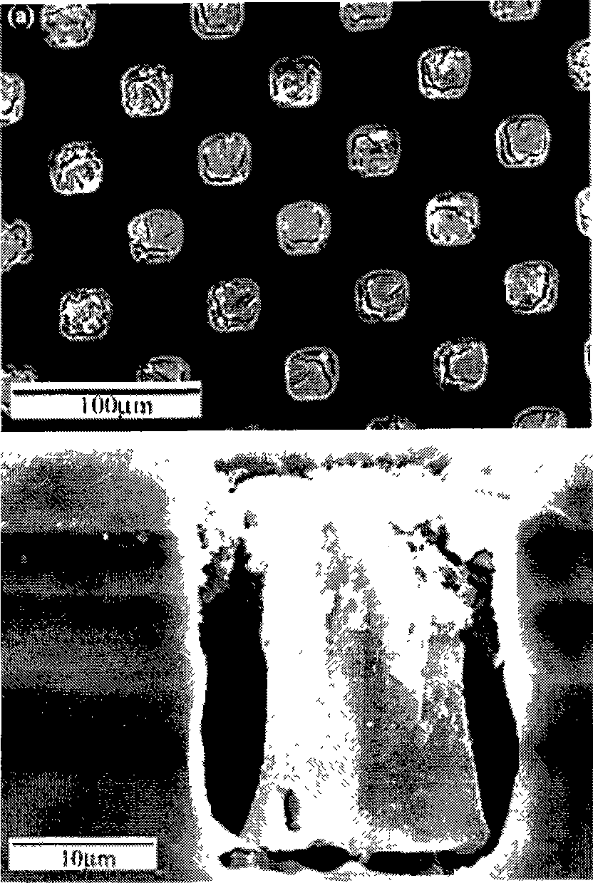
[0038] As in Example 1, the metal alkoxide reflux method was used to obtain 0.4M KNN sol, which was filled into a silicon template with a pore length, a pore width of 20 μm, a pore depth of 30 μm, and a pore spacing of 42 μm under reduced pressure. After the solution treatment, the annealing treatment was carried out at 830° C., and finally the silicon around the microcolumn was removed by RIE method to obtain the KNN microcolumn array. Use the scanning probe system (SPI4000) to test its displacement-voltage curve, which proves the piezoelectricity of the KNN microcolumn, d 33 24pC / N as Figure 5 . The epoxy resin is filled into the microcolumn gap of the array to obtain the piezoelectric ceramic array structure composite material, and its surface morphology is as follows: Figure 6 shown.
Embodiment 3
[0040] As in Example 1, the same KNN sol and a silicon template with a pore length, a pore width of 10 μm, a pore depth of 30 μm, and a pore spacing of 30 μm were used. Under the condition of mechanical pump vacuuming, use the sol to repeatedly fill the silicon template and pyrolyze it at 400°C for three times. After annealing at 830°C, the silicon around the KNN microcolumn is etched to remove the column length, width 7 μm, height 20 μm, A KNN microcolumn array with a row spacing of 30 μm, such as Figure 7 .
PUM
| Property | Measurement | Unit |
|---|---|---|
| width | aaaaa | aaaaa |
Abstract
Description
Claims
Application Information


