Dielectrically isolated integrated circuit silicon chip and preparation method thereof

A dielectric isolation and integrated circuit technology, applied in the field of dielectric isolation silicon wafers and its preparation, can solve the problems of parasitic radiation resistance, poor isolation performance, and no performance, so as to shorten the high temperature time, improve circuit performance, and crystal structure. full effect

Inactive Publication Date: 2009-06-24
TIANSHUI HUATIAN MICROELECTRONICS
View PDF0 Cites 2 Cited by
  • Summary
  • Abstract
  • Description
  • Claims
  • Application Information

AI Technical Summary

Problems solved by technology

In this process, the isolation performance deteriorates with the increase of temperature. The PNP tube can only be made into a horizontal PNP tube. The performance is not as good as that of the vertical PNP tube. There are parasitic effects and poor radiation resistance, which affects the application in some special requirements. application

Method used


Image

  • Dielectrically isolated integrated circuit silicon chip and preparation method thereof
  • Dielectrically isolated integrated circuit silicon chip and preparation method thereof
  • Dielectrically isolated integrated circuit silicon chip and preparation method thereof

Examples


Embodiment 1

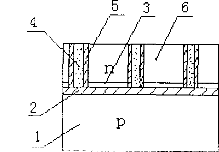
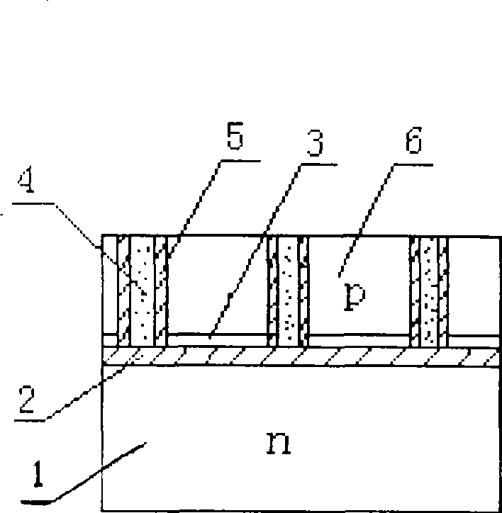
[0032] Example 1, see figure 1 , a kind of N-type dielectric isolation integrated circuit silicon chip, has P-type substrate silicon single wafer 1, is provided with sandwich oxide layer 2 on it, also has N-type silicon single crystal layer 6, is provided with in silicon single crystal layer 6 Buried layer 3; its silicon single crystal layer 6 is separated into mutually insulated isolation squares by silicon dioxide 5, polysilicon 4 and sandwich oxide layer 2. The thickness of the N-type silicon single crystal layer 6 is 5-16 μm; the N-type sheet resistance is 6-15Ω / □.

Embodiment 2

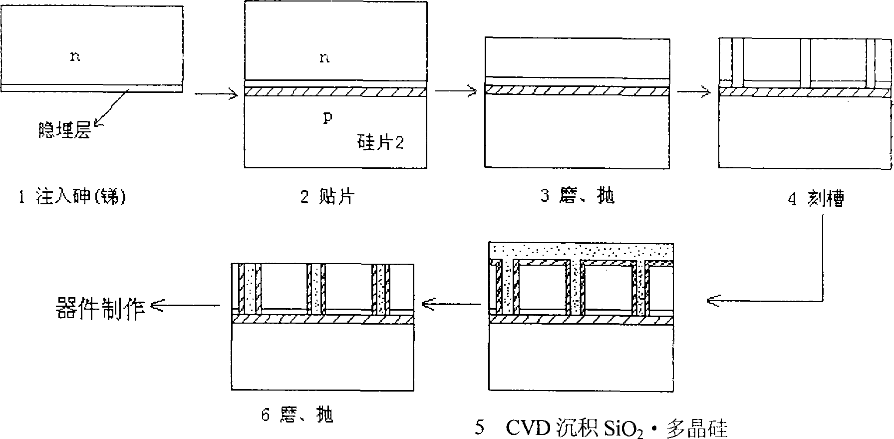
[0034] Example 2, see figure 2 , the preparation method of the N-type dielectric isolation integrated circuit silicon chip, the steps of its preparation are:

[0035] (1)N + Buried layer preparation: high concentration of arsenic (N type) 8 x 10 on the polished surface of N type 0.5-6.0Ωcm single crystal silicon wafer 19 —10 20 / cm 3 Ion implantation, after high temperature annealing, the temperature is 25-1250 ℃, N + The buried layer sheet resistance is controlled at 6-15Ω / □, the junction depth is controlled at 2.0-3.0μm, and the formation of N + For the buried layer, the substrate temperature of the implantation process is 400-700°C, the implantation energy is 100-150kev, and the dose is 10 15 —10 16 cm 2 ;

[0036] (2) SMD: The polished surface of another P-type 6-10Ωcm oxidized silicon wafer without a buried layer and the N + The polished surface of the N-type silicon wafer buried layer of the buried layer is correspondingly pasted together for oxidation at a tempe...

Embodiment 3

[0041] Example 3, see figure 2 , the preparation method of the N-type dielectric isolation integrated circuit silicon chip, the steps of its preparation are:

[0042] The preparation method of the N-type dielectric isolation integrated circuit epitaxial wafer, the step (1) of its preparation also includes: forming N + After the buried layer, a local high boron concentration of 2-8×10 19 / cm 3 Ion implantation, after high temperature annealing, the temperature is 25-1250 ℃, the sheet resistance is controlled at 8-20Ω / □, the junction depth is controlled at 2.0-3.0μm; the formation of P + For the buried layer, the substrate temperature of the implantation process is 400-700°C, the implantation energy is 100-150kev, and the dose is 10 15 —10 16 / cm 2 .

[0043] All the other steps are the same as in Example 2.


PUM


Abstract

The invention mainly relates to a preparation method of a dielectric isolation silicon chip. An N-type / P-type dielectric isolation integrated circuit silicon chip is mainly characterized in that the integrated circuit silicon chip is provided with an N-type / P-type substrate silicon chip (1) and an N-type / P-type silicon monocrystal layer (6); a sandwiched oxide layer (2) is arranged on the N-type / P-type substrate silicon chip (1); a buried layer (3) is arranged inside the silicon monocrystal layer (6); the silicon monocrystal layer (6) is separated into mutually insulated isolation cubic blocks through silicon dioxide (5), polysilicon (4) and the sandwiched oxide layer (2). The invention also discloses a preparation method of the N-type / P-type dielectric isolation integrated circuit silicon chip; and the method comprises the steps of buried layer preparation, patching, grinding, polishing and grooving. Because the high-temperature time is greatly shortened in the preparation, the crystal structure is more integrated and the process control is more accurate, and high-performance circuits with special requirements can be produced. The resistivity of the single chip is appropriately increased, so that high (power)-voltage circuits can be produced with a certain power output.

Description

Technical field: [0001] The invention mainly relates to a dielectric isolation silicon wafer and a preparation method thereof, and belongs to the technical field of integrated circuits. Background technique: [0002] In the manufacture of bipolar analog integrated circuits, the monolithic PN junction isolation epitaxial wafer method is generally used to manufacture. In the case of higher reliability requirements and harsher working environment conditions, the circuit manufactured by using PN junction isolation epitaxial method is subject to certain restrictions, and the performance of analog integrated circuits manufactured with dielectric isolation silicon wafers is significantly better than the former. With the development of human beings into deep space exploration, the requirements for radiation resistance and high and low temperature resistance of electronic products are getting higher and higher. [0003] SOI technology is internationally recognized as "silicon-based ...

Claims


Application Information

Patent Timeline
Patent Type & Authority Applications(China)
IPC IPC(8): H01L27/12H01L21/84H01L21/76
Inventor 周鸣新
Owner TIANSHUI HUATIAN MICROELECTRONICS
Why Eureka
Try Eureka