Nickel protoxide / silicon nano-wire and use thereof for preparing integrated super capacitor electrode material

A technology of silicon nanowires and nickel oxide, which is applied in capacitors, electrolytic capacitors, nanostructure manufacturing, etc., can solve the problems of incompatibility of integrated circuit technology, increase of collector layer resistance, and difficult use of active materials, etc., and achieve good charging Discharge characteristics, low equivalent internal resistance, low cost effect

Inactive Publication Date: 2011-02-02
EAST CHINA NORMAL UNIV
View PDF0 Cites 0 Cited by
  • Summary
  • Abstract
  • Description
  • Claims
  • Application Information

AI Technical Summary

Problems solved by technology

[0004] In the prior art, carbon nanotubes or activated carbon are generally used as substrates, on which transition metal oxides such as manganese oxide, nickel oxide, and ruthenium oxide are prepared as active materials for supercapacitor electrodes; wherein the supercapacitor electrodes based on ruthenium oxide The material has the best supercapacitive properties, but it is expensive; in addition, other transition metal oxide supercapacitor electrode materials based on activated carbon or carbon nanotubes as the carrier can obtain a large specific surface area, but because the outside is completely covered The surface is covered with transition metal oxides, which leads to an increase in the resistance of the current collector layer, and it is difficult to fully utilize the active material; it has been reported that depositing nickel oxide on the surface of carbon nanotubes can obtain nickel oxide / carbon with high supercapacitive performance. Nanotube structure, but its preparation method is not compatible with integrated circuit process

Method used


Image

  • Nickel protoxide / silicon nano-wire and use thereof for preparing integrated super capacitor electrode material
  • Nickel protoxide / silicon nano-wire and use thereof for preparing integrated super capacitor electrode material
  • Nickel protoxide / silicon nano-wire and use thereof for preparing integrated super capacitor electrode material

Examples


Embodiment 1

[0030] (1). Fabrication of silicon nanowires (SiNWs) by chemical wet etching

[0031] (a) Choose N-type (100 crystal orientation, resistivity 0.06-0.2Ω·cm) single-sided polished silicon wafer, cut into 1cm×1cm sample, clean with RCA standard procedure; The surface is pretreated in a hydrofluoric acid solution for 3-5 minutes to activate the surface, and then etched in an etching solution containing 35 mM silver nitrate and 20% by mass of hydrofluoric acid for 50 minutes.

[0032] (b) Use a nitric acid solution with a mass concentration of 30% to remove residual silver particles on the surface of the silicon nanowires, then fully wash them with deionized water, and dry them in a drying oven at 70° C. to 80° C. for later use.

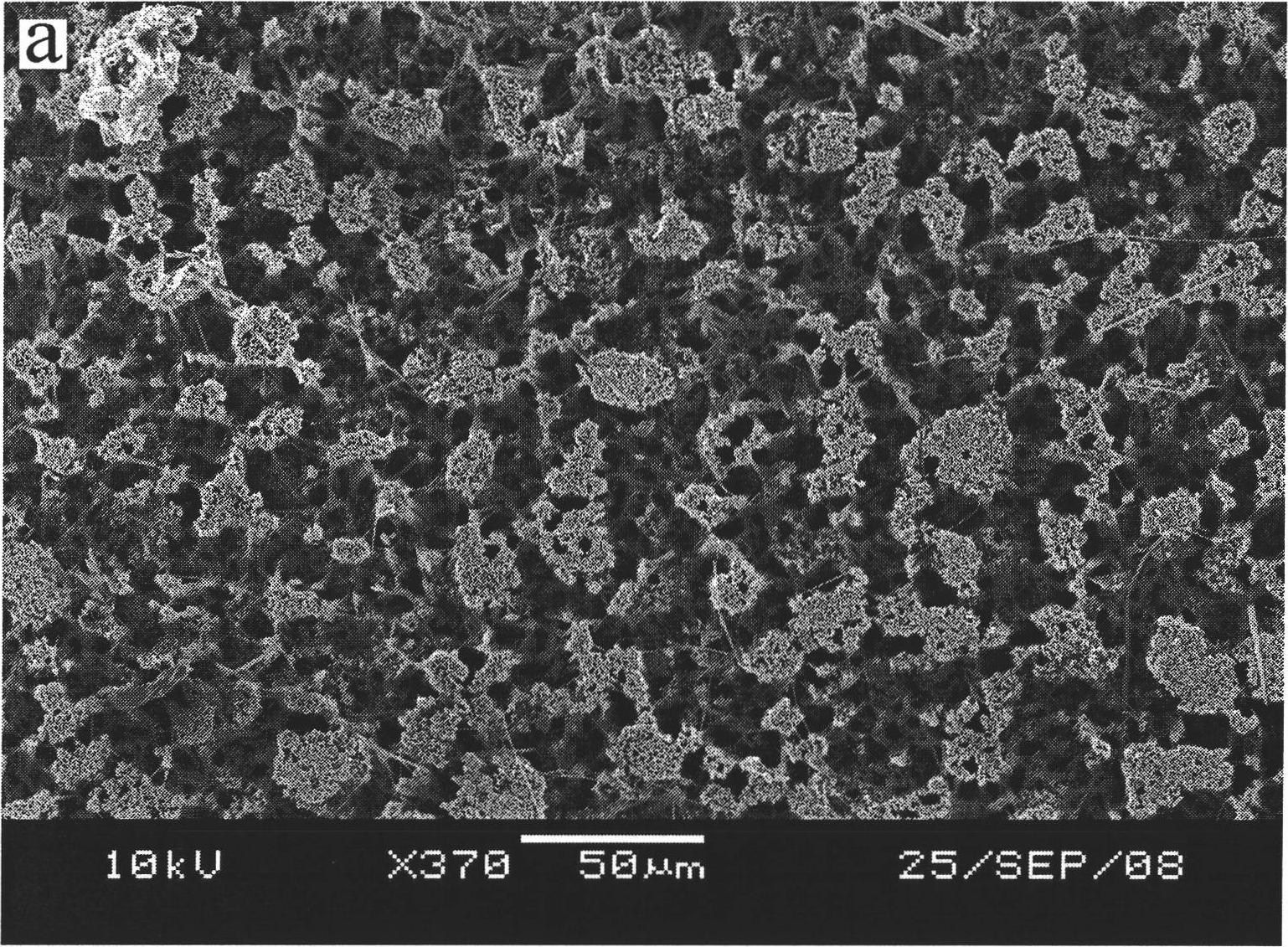
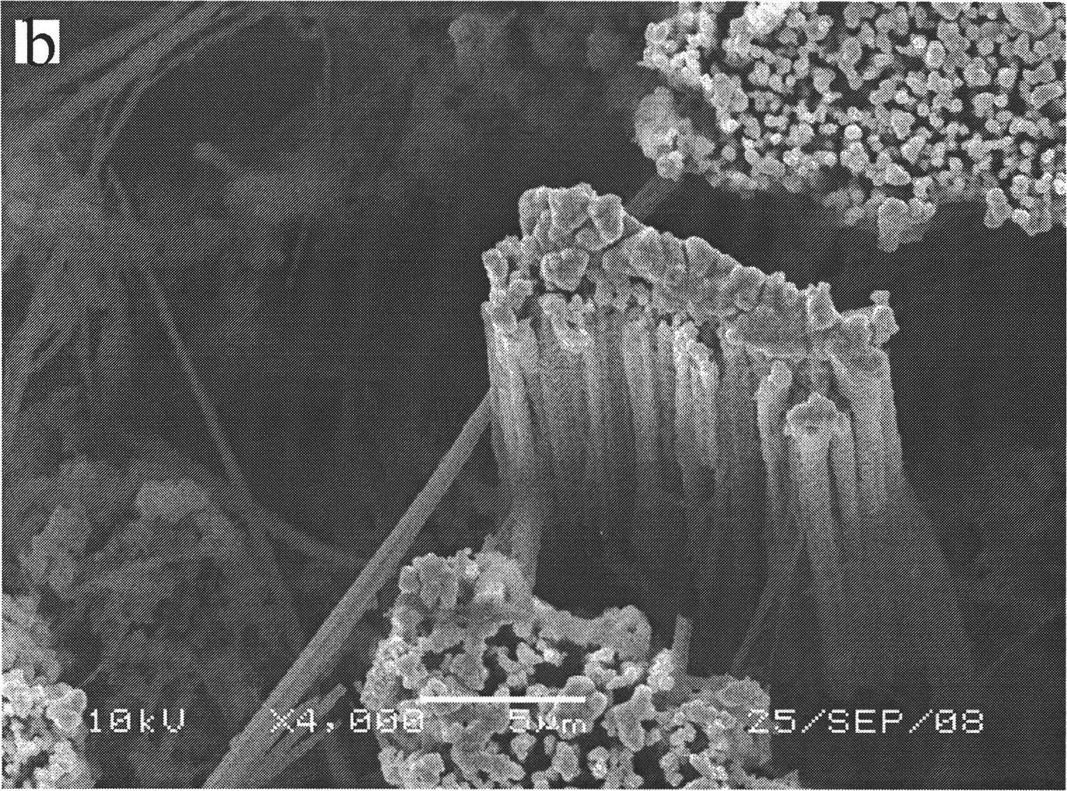
[0033] The resulting silicon nanowires had an average diameter of ~80 nm and a length of ~200 m.

[0034] (2). Electroless deposition of nickel thin layer to make nickel-silicon nanowire composite (Ni-SiNWs). The SiNWs prepared above were pretreated with...

Embodiment 2

[0042] (1). Fabrication of silicon nanowires (SiNWs) by chemical wet etching

[0043] (a) Choose N-type (100 crystal orientation, resistivity 0.06-0.2Ω·cm) single-sided polished silicon wafer, cut into 1cm×1cm sample, clean with RCA standard procedure; The surface is pretreated in an acid solution for 3-5 minutes to activate the surface, and then etched in an etching solution containing 20 mM silver nitrate and 15% by mass hydrofluoric acid for 30 minutes.

[0044] (b) Use concentrated nitric acid solution with a mass concentration of 35% to remove residual silver particles on the surface of the silicon nanowires, then fully wash with deionized water, and dry in a drying oven at 70° C. to 80° C.

[0045] The resulting silicon nanowires had an average diameter of ~200 nm and a length of ~50 μm.

[0046] (2). Electroless deposition of nickel thin layer to make nickel-silicon nanowire composite

[0047] The SiNWs prepared above were pretreated with 1% sodium dodecylbenzenesulfo...

Embodiment 3

[0052] (1). Fabrication of silicon nanowires (SiNWs) by chemical wet etching

[0053] (a) Choose N-type (100 crystal orientation, resistivity 0.06-0.2Ω·cm) single-sided polished silicon wafer, cut into 1cm × 1cm sample, clean with RCA standard procedure; The surface is pretreated in an acid solution for 3-5 minutes to activate the surface, and then etched in a solution containing 25 mM silver nitrate and 15% by mass of hydrofluoric acid for 30 minutes.

[0054] (b) Use concentrated nitric acid solution with a mass concentration of 30% to remove residual silver particles on the surface of the silicon nanowires, then fully wash with deionized water, and dry in a drying oven at 70°C to 80°C.

[0055] The resulting silicon nanowires had an average diameter of ~150 nm and a length of ~100 μm.

[0056] (2). Electroless deposition of nickel thin layer to make nickel-silicon nanowire composite

[0057] The SiNWs prepared above were pretreated with 1% sodium dodecylbenzene sulfonate ...


PUM

PropertyMeasurementUnit
diameteraaaaaaaaaa
lengthaaaaaaaaaa
electrical resistivityaaaaaaaaaa

Abstract

The invention discloses a NiO / SiN wire and a method for preparing an integrated supercapacitor electrode material with high performance by adopting the material. The preparation method comprises the following steps: (1) the SiN wire is taken as a framework, a nickel membrane is sedimented on the SiN wire by the electroless plating technique to produce a nickel-silicon nanometer wire composite; and (2) the produced nickel-silicon nanometer wire composite is subject to rapid thermal annealing oxidation treatment. The invention adopts the advantages of the SiN wire that the scale is small, the specific surface is large, the surface atom has a large amount of nonsaturated bonds, and the tensiometric property is great, and takes the SiN wire as the framework for loading the NiO nanometer structure. The NiO / SiN wire has high specific capacitance, low equivalent essential resistance and good charging and discharging properties, is compatible with the integrated circuit technique and can be used for preparing the integrated supercapacitor electrode material with high performance.

Description

technical field [0001] The invention belongs to the field of electrochemical capacitor materials, and relates to a method of preparing nickel oxide / silicon nanowires (NiO / SiNWs) on silicon nanowires by electroless nickel plating and thermal oxidation annealing, and using the nickel oxide / silicon nanowires Nanowires are used as electrode materials for integrable supercapacitors. Background technique [0002] Due to the small size, large specific surface area, and large number of unsaturated bonds on the surface atoms of silicon nanowires, silicon nanowires have strong surface activity. NiO / SiNWs high-performance supercapacitor electrode materials can be prepared by using it as a framework for loading NiO nanostructures. [0003] The nano-NiO structure is one of the known transition metal oxides that can be used as electrode materials for supercapacitors. Although its supercapacitive performance is slightly lower than that of RuO materials, its preparation process is simple an...

Claims


Application Information

Patent Timeline
Patent Type & Authority Patents(China)
IPC IPC(8): B82B1/00H01G9/042
CPCY02E60/13
Inventor 陶佰睿苗凤娟李辉麟姚伟陈雪皎张健
Owner EAST CHINA NORMAL UNIV
Why Eureka
Try Eureka