

Method for reducing 4H-SiC intrinsic deep energy level defects
A deep-level and defect technology, applied in the field of microelectronic materials and devices, can solve the problems of lack of consideration of temperature and surface protection, affecting the quality of 4H-SiC single crystal, and unable to effectively reduce deep-level defects, so as to reduce damage. , the effect of reducing the precipitation of Si
- Summary
- Abstract
- Description
- Claims
- Application Information
AI Technical Summary
Problems solved by technology
Method used
Image

Examples
Embodiment 1
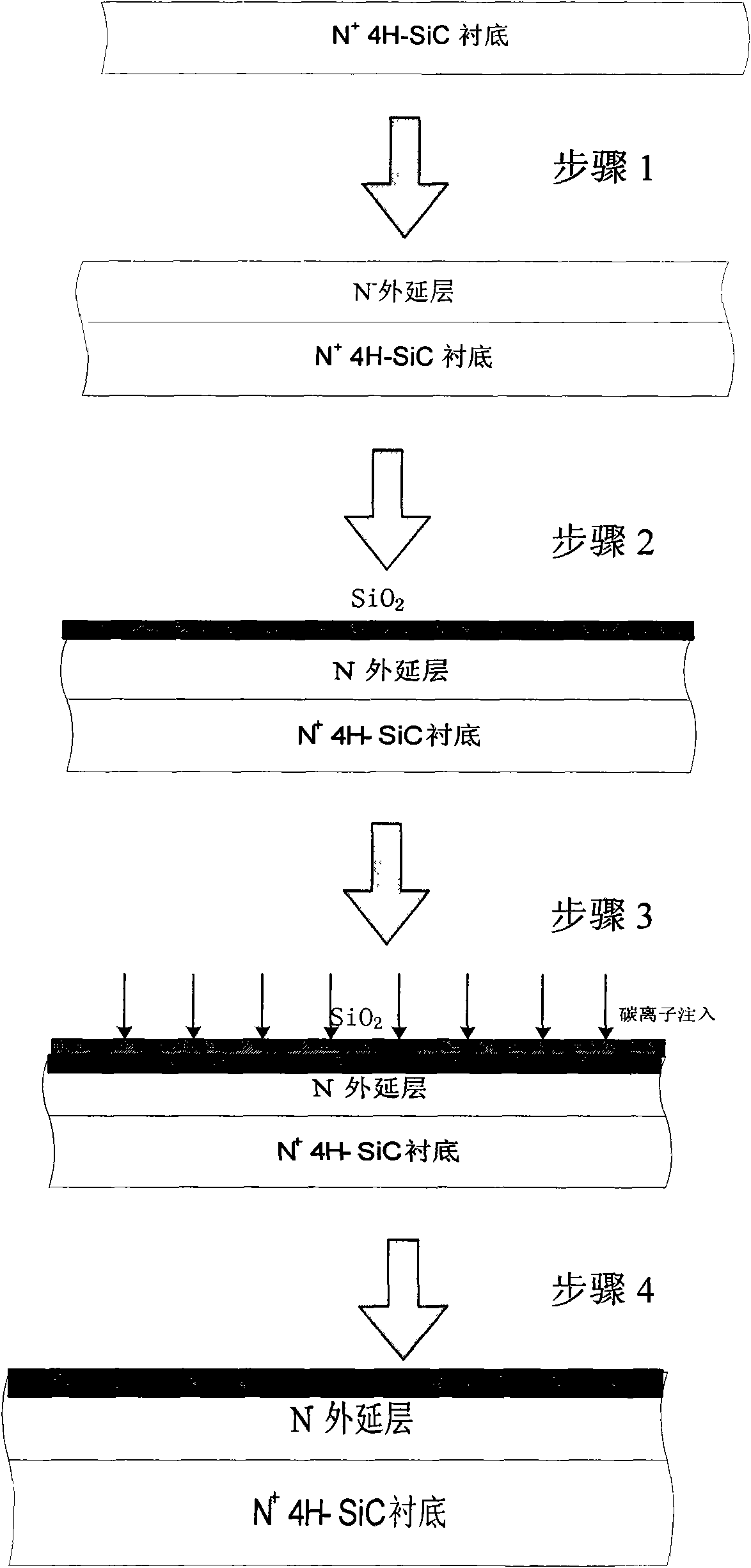
[0026] refer to figure 1 , the present invention comprises the following steps:
[0027] Step 1, pretreating the used 4H-SiC material.
[0028] Using 4H-SiC material produced by CREE company, its doping level is 10 18 cm -3 . First, passivate the surface of the 4H-SiC substrate with molten KOH, the etching temperature is 210°C, and the etching time is 15s; then, the passivated wafer is cleaned with acetone, methanol, and deionized water in sequence Clean; finally, use RCA standard cleaning process to remove the oxide layer on the surface of the sample.
[0029] Step 2, grow N on the substrate - epitaxial layer.
[0030] Homogeneous N was grown by CVD on pretreated substrates - type epitaxial layer, the epitaxial layer doping is 1.1×10 15 cm -3 , with a thickness of 10 ± 0.1 μm.
[0031] In step 3, the ion implantation barrier layer is fabricated by a deposition method.
[0032] After the epitaxial wafer is cleaned by RCA standard, 100nm SiO2 is formed on the front o...
Embodiment 2
[0040] refer to figure 1 , the present invention comprises the following steps:
[0041] Step 1, pretreating the used 4H-SiC material.
[0042] Using 4H-SiC material produced by CREE company, its doping level is 10 18 cm -3 . First, passivate the surface of the 4H-SiC substrate with molten KOH, the etching temperature is 210°C, and the etching time is 15s; then, the passivated wafer is cleaned with acetone, methanol, and deionized water in sequence Clean; finally, use RCA standard cleaning process to remove the oxide layer on the surface of the sample.
[0043] Step 2, grow N on the substrate - epitaxial layer.
[0044] Homogeneous N was grown by CVD on pretreated substrates - type epitaxial layer, the epitaxial layer doping is 1.1×10 15cm -3 , with a thickness of 10 ± 0.1 μm.
[0045] In step 3, the ion implantation barrier layer is fabricated by a deposition method.
[0046] After the epitaxial wafer is cleaned by RCA standard, 200nm SiO2 is formed on the front of...
Embodiment 3
[0054] refer to figure 1 , the present invention comprises the following steps:
[0055] Step 1, pretreating the used 4H-SiC material.
[0056] Using 4H-SiC material produced by CREE company, its doping level is 10 18 cm -3 . First, passivate the surface of the 4H-SiC substrate with molten KOH, the etching temperature is 210°C, and the etching time is 15s; then, the passivated wafer is cleaned with acetone, methanol, and deionized water in sequence Clean; finally, use RCA standard cleaning process to remove the oxide layer on the surface of the sample.
[0057] Step 2, grow N on the substrate - epitaxial layer.
[0058] Homogeneous N was grown by CVD on pretreated substrates - type epitaxial layer, the epitaxial layer doping is 1.1×10 15 cm -3 , with a thickness of 10 ± 0.1 μm.
[0059] In step 3, the ion implantation barrier layer is fabricated by a deposition method.
[0060] After the epitaxial wafer is cleaned by RCA standard, 100nm SiO2 is formed on the front o...
PUM
 Abstract
Description
Claims
Application Information