Low-temperature growth method of silicon quantum dots for solar battery

A technology of silicon quantum dots and solar cells, applied in circuits, electrical components, sustainable manufacturing/processing, etc., can solve the problems of increased process complexity and production costs, poor controllability and repeatability of the growth process, thermal damage of solar cells, etc. problem, to achieve the effect of good process controllability and repeatability, good uniformity and fast deposition speed

Inactive Publication Date: 2010-01-13
YUNNAN NORMAL UNIV
View PDF0 Cites 16 Cited by
  • Summary
  • Abstract
  • Description
  • Claims
  • Application Information

AI Technical Summary

Problems solved by technology

Generally, if the first method is adopted, high-temperature post-annealing (about 1100°C) treatment is essential, which will increase the complexity of the process and production costs, and may also cause thermal damage to the solar cell; the second method does not Requires post-annealing, but is very difficult, and the growth process is less controllable and reproducible

Method used


Image

  • Low-temperature growth method of silicon quantum dots for solar battery

Examples


Embodiment 1

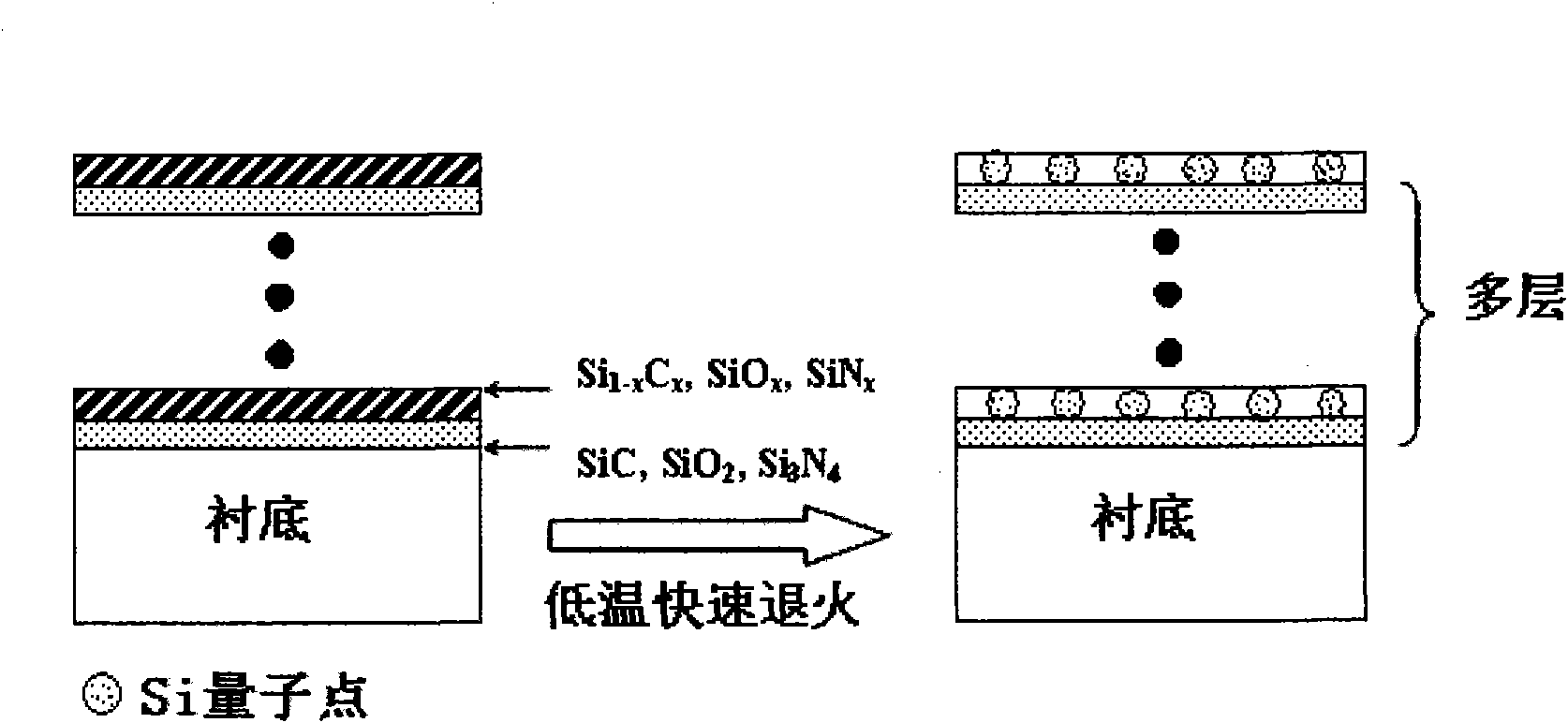
[0015] Using radio frequency plasma enhanced chemical vapor deposition technology, the substrate chooses a Si sheet with a diameter of 4 inches and a thickness of 1mm, and alternately grows 2nm thick Si 3 N 4 Dielectric layer and 2nm Si-rich SiN x layer, Si 3 N 4 / SiN x The deposition period is 40. Deposition conditions: RF frequency 13.56MHz, RF power 60W, background vacuum up to 1×10 -4 Pa, the reaction gas is N 2 Diluted SiH 4 (gas volume N 2 : SiH 4 =1:1) and NH 3 , the working pressure is 10Pa, the deposition temperature is 300℃, and the deposited Si 3 N 4 When the medium layer is used, the reaction gas flow rate is N 2 Diluted SiH 4 30sccm (standard condition milliliter per minute), NH 3 30sccm, deposition rate 0.2nm / s, deposition of Si-rich SiN x layer, the reaction gas flow rate is N 2 Diluted SiH 4 100sccm, NH 3 The deposition rate is 30sccm, and the deposition rate is 0.25nm / s; the film sample is placed in a rapid photothermal treatment furnace for ...

Embodiment 2

[0017] Microwave plasma-enhanced chemical vapor deposition technology is adopted, and the substrate is selected as a 20cm×20cm, 3mm thick ordinary glass sheet, and 2nm thick SiO is alternately grown 2 Dielectric layer and 4nm Si-rich SiN x layer, SiO 2 / SiN x The deposition period is 50. Deposition conditions: RF frequency 13.56MHz, RF power 60W, background vacuum up to 1×10 -4 Pa, the reaction gas is N 2 Diluted SiH 4 (gas volume N 2 : SiH 4 =1:1) and O 2 , the working pressure is 10Pa, the deposition temperature is 300℃, and the SiO 2 When the medium layer is used, the reaction gas flow rate is N 2 Diluted SiH 4 For 30sccm (standard condition milliliters per minute), O 2 30sccm, deposition rate 0.2nm / s, deposition of Si-rich SiN x layer, the reaction gas flow rate is N 2 Diluted SiH 4 100sccm, NH 3 The deposition rate is 30 sccm, and the deposition rate is 0.25nm / s; the thin film sample is placed in a rapid photothermal treatment furnace for annealing treatmen...

Embodiment 3

[0019]Electron cyclotron resonance plasma-enhanced chemical vapor deposition technology is used, the substrate is 20cm×30cm, 2mm thick stainless steel sheet, and 3nm thick SiC dielectric layer and 6nm Si-rich SiN are alternately grown x layer, SiC / SiN x The deposition period is 60. Deposition conditions: RF frequency 13.56MHz, RF power 60W, background vacuum up to 1×10 -4 Pa, the reaction gas is N 2 Diluted SiH 4 (gas volume N 2 : SiH 4 =1:1) and CH 4 , the working pressure is 10Pa, the deposition temperature is 300℃, when depositing the SiC dielectric layer, the reaction gas flow rate is N 2 Diluted SiH 4 30sccm (standard condition milliliters per minute), CH 4 30sccm, deposition rate 0.2nm / s, deposition of Si-rich SiN x layer, the reaction gas flow rate is N 2 Diluted SiH 4 100sccm, NH 3 The deposition rate is 30sccm, and the deposition rate is 0.25nm / s; the film sample is placed in a rapid photothermal treatment furnace for annealing treatment, using a halogen t...


PUM

PropertyMeasurementUnit
diameteraaaaaaaaaa
thicknessaaaaaaaaaa
particle diameteraaaaaaaaaa

Abstract

The invention relates to a low-temperature growth method of silicon quantum dots for a solar battery, which belongs to the technical field of silicon quantum dot material. The method comprises the following steps: alternately growing a silicon compound dielectric layer of the stoichiometric proportion and a silicon compound layer containing Si which is several nanometers thick in stoichiometric ratio on a silicon wafer or a quartz sheet or a glass sheet or a stainless steel sheet or high-temperature resistant polymer substrate material at the temperature lower than 450 DEG C by using the plasma chemical vapour deposition (PCVD) technology; carrying out post annealing treatment at the temperature lower than or equal to 550 DEG C by using the rapid photo-thermal annealing technology, so that the residual Si in the silicon compound layer containing Si generates diffusion transfer and solid phase crystallization to form the Si quantum dots, wherein the formed Si quantum dots are arranged in a layered mode, the size of each Si quantum dot is controlled by the thickness of the originally-grown silicon compound layer containing Si, and the density of each Si quantum dot is determined by the content of Si in the original SiN<x> layer containing Si. The invention has the advantages of low depositing temperature, quick speed and good technology controllability and repeatability, thus the uniformity of the grown silicon quantum dot material is good; and the invention is favorable for integrated manufacture and cost reduction of devices.

Description

Technical field: [0001] The invention relates to a low-temperature growth method of silicon quantum dots for solar cells, belonging to the technical field of silicon quantum dot materials. Background technique: [0002] In order to enhance the competitiveness with conventional energy sources, high-efficiency, low-cost and long-life solar cells have always been the goal pursued by people. The current commercial solar cells are mainly the first-generation solar cells based on silicon wafers. This technology has matured, and its photoelectric conversion efficiency is also close to the physical limit, but its cost is increasingly constrained by the raw material (ie, silicon wafers) itself. In the past 20 years, the second-generation solar cells based on semiconductor thin film materials have developed vigorously. Due to the adoption of thin film deposition technology, compared with the first generation of solar cells, the cost of the second generation of solar cells is greatly ...

Claims


Application Information

Patent Timeline
Patent Type & Authority Applications(China)
IPC IPC(8): H01L31/18
CPCY02P70/50
Inventor 杨培志刘黎明郝瑞亭杨雯莫镜辉邓书康
Owner YUNNAN NORMAL UNIV
Why Eureka
Try Eureka