Etching method

A main etching and over-etching technology, applied in the direction of electrical components, semiconductor/solid-state device manufacturing, circuits, etc., can solve the problems of uneven etching lines, offset or weaken the PR-loading effect, and no micro-loading effect, etc. achieve the effect of improving uniformity

Active Publication Date: 2010-07-14
BEIJING NAURA MICROELECTRONICS EQUIP CO LTD
View PDF1 Cites 6 Cited by
  • Summary
  • Abstract
  • Description
  • Claims
  • Application Information

AI Technical Summary

Problems solved by technology

[0011] For those etch processes that do not easily generate polymers, such as using Cl 2 and O 2 In the process of etching gas, there is no obvious micro-loading effect. In this case, the main etching step cannot be used to offset or weaken the PR-loading effect, resulting in the problem of uneven etching lines.

Method used


Image

  • Etching method
  • Etching method
  • Etching method

Examples


Embodiment 1

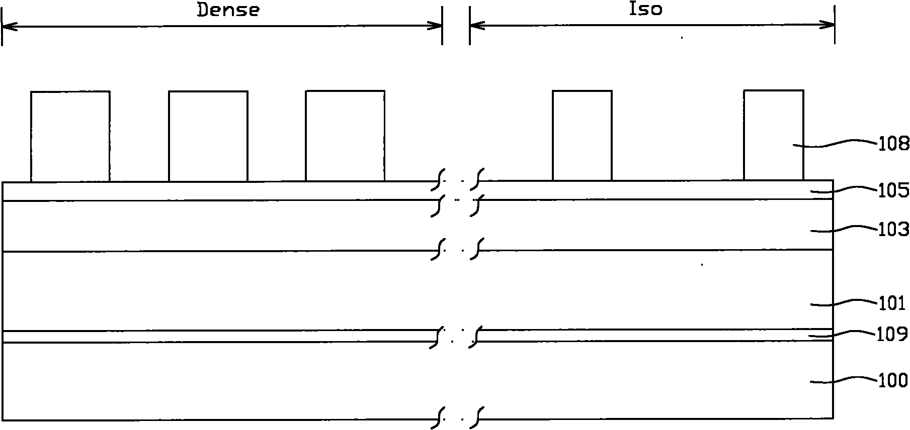
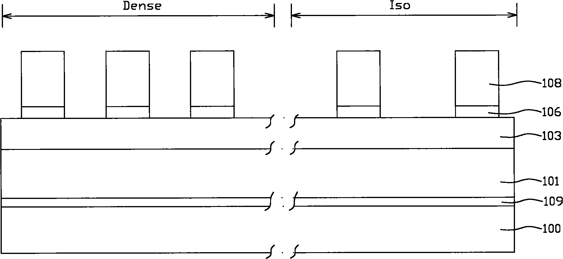
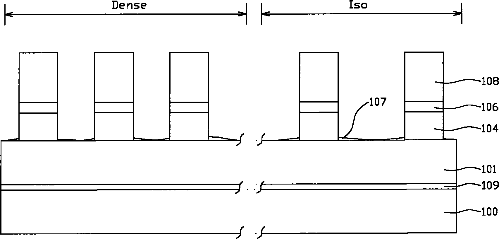
[0044] Generally, the gate structure of a Dynamic Random-Access Memory (DRAM) is a composite gate composed of polysilicon and metal silicide, for example, a stacked gate with tungsten silicide as the upper layer and doped polysilicon as the lower layer. In this embodiment, the etching method will be described in detail with the background of the forming process of the gate structure of the DRAM.

[0045] Figure 1 to Figure 5 It is a schematic diagram of the etching method described in this implementation, Figure 6 It is a flowchart of the etching method.

[0046] The etching method includes:

[0047] refer to figure 1 As shown, as in step S1, a semiconductor wafer 100 is provided, and the semiconductor wafer 100 may include elemental semiconductors, such as silicon or silicon germanium (SiGe) of single crystal, polycrystalline or amorphous structure, and may also include compound semiconductors, such as silicon carbide , indium antimonide, lead telluride, indium arsenide...

Embodiment 2

[0068] Different from DRAM, usually the gate structure of metal oxide semiconductor (Metal Oxide Semiconductor, MOS) device is only one layer of polysilicon gate. The etching method described above will be described.

[0069] Figure 9 to Figure 12 It is a schematic diagram of the etching method described in this implementation.

[0070] The etching method includes:

[0071] refer to figure 1 As shown, a semiconductor wafer 200 is provided, and the semiconductor wafer 200 has active regions (not shown) for forming source and drain electrodes of MOS devices, and shallow regions for isolating and insulating different active regions. Trench isolation structure (not shown in the figure), the composition of the semiconductor wafer 200 is the same as that of Embodiment 1, and may include elemental semiconductors or compound semiconductors, which will not be listed one by one;

[0072] The exposed surface of the semiconductor wafer 200 is covered with a gate dielectric layer 209...


PUM


Abstract

The invention provides an etching method, which comprises steps of primary etching, main etching and over etching; and in the primary etching, the mixed gas of fluorine-based gas and chlorine-based gas forms plasmas, wherein the fluorine-based gas is one or combination of at least two of CF4, Ch2F2 and CHF3; and the chlorine-based gas is one or combination of at least two of Cl2, CH2Cl2 and CH3Cl. In the etching method, the chlorine-based gas serving as the etching gas is increased in the primary etching step, so that the shrinkage of the line width of lines of patterns in a Dense area is greater than that of the line width of lines of patterns in an Iso area, which is opposite to a condition that the line width of the lines of the patterns in the Dense area is greater than that in the Iso area caused by the PR-loading effect; therefore, the influence of the PR-loading effect on the line width uniformity is compensated finally, and uniform AEI line width is obtained at each position of a semiconductor chip.

Description

technical field [0001] The invention relates to the technical field of integrated circuit manufacturing, in particular to an etching method. Background technique [0002] In the integrated circuit manufacturing process, the photoresist layer (photoresist, PR) covering the semiconductor substrate is exposed by photolithography technology, and a patterned photoresist layer is formed after development, and then photoresist layer is formed by etching technology. The circuit pattern in the glue layer is transferred to the semiconductor substrate to form an integrated circuit structure. [0003] In the integrated circuit manufacturing process with a feature size above 0.35 microns, an I-line light source with a wavelength of 365nm is usually used for exposure to save the cost of lithography. Correspondingly, the photoresist layer exposed by this light source uses a positive I-line Photoresists such as diazonaphthoquinone novolaks. [0004] During actual exposure, in order to red...

Claims


Application Information

Patent Timeline
Patent Type & Authority Applications(China)
IPC IPC(8): H01L21/00H01L21/02H01L21/28
Inventor 白志民
Owner BEIJING NAURA MICROELECTRONICS EQUIP CO LTD
Why Eureka
Try Eureka