Method for preparing spherical cadmium sulfide (CdS) semiconductor film

A semiconductor and thin film technology, which is applied in the field of preparing CdS thin films, can solve the problems of high equipment requirements, complex processes, expensive equipment and instruments, etc., and achieve the effects of good uniformity, high film purity, and simple process equipment

Inactive Publication Date: 2010-09-29
SHAANXI UNIV OF SCI & TECH
View PDF2 Cites 8 Cited by
  • Summary
  • Abstract
  • Description
  • Claims
  • Application Information

AI Technical Summary

Problems solved by technology

However, these methods either have high requirements on equipment, expensive equipment and instruments, and the supporting facilities and required raw m...

Method used


Image

  • Method for preparing spherical cadmium sulfide (CdS) semiconductor film
  • Method for preparing spherical cadmium sulfide (CdS) semiconductor film

Examples


Embodiment 1

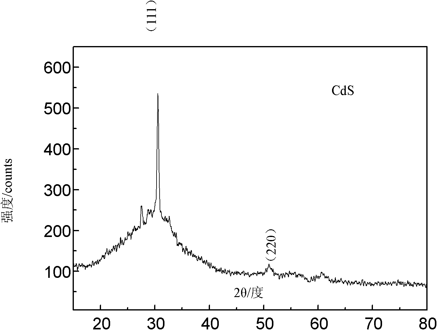
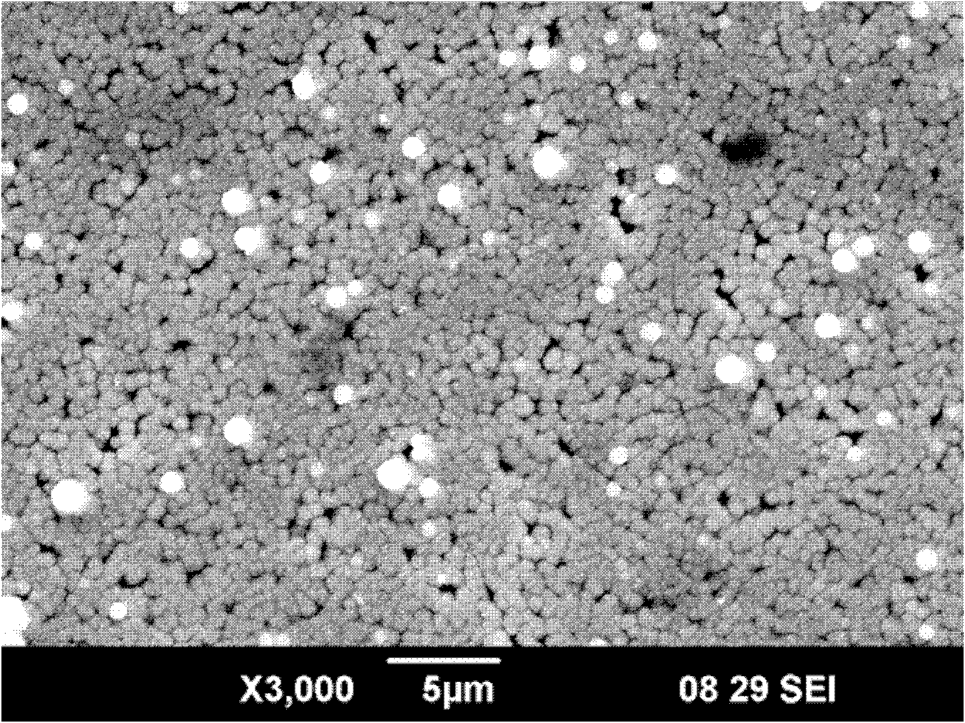
[0011] Embodiment 1: 1) get 0.06mmol analytically pure cadmium acetate (C 4 h 6 CdO 4 ) is placed in a beaker, then in the beaker, add 5mL oleic acid dropwise and stir evenly, then add 40mL distilled water, and obtain a uniform solution A after ultrasonic dispersion; 2) add 0.6mmol analytically pure sodium thiosulfate pentahydrate ( Na 2 S 2 SO 3 ·5H 2 0) add distilled water again to make the total volume of the solution be 100mL and keep stirring, and obtain solution B after ultrasonic dispersion; 3) add analytically pure film-forming aid polyvinylpyrrolidone (PVP) to the B solution, so that the concentration of PVP is 0.005 mol / L, using HCl solution to adjust the pH value to 2.5 and form a uniform sol C after ultrasonication; 4) Clean the ITO glass with ultrasonic vibration in water and absolute ethanol respectively, and then in 70% sol with a volume ratio of 1:1 Nitric acid and a concentration of 30% hydrogen peroxide in the activation solution soak activation treatme...

Embodiment 2

[0013] Embodiment 2: 1) get 0.08mmol analytically pure cadmium acetate (C 4 h 6 CdO 4 ) is placed in a beaker, then in the beaker, add 5mL oleic acid dropwise and stir evenly, then add 40mL distilled water, and obtain a uniform solution A after ultrasonic dispersion; 2) add 1.2mmol analytically pure sodium thiosulfate pentahydrate ( Na 2 S 2 SO 3 ·5H 2 0) add distilled water again to make the solution total volume be 100mL and keep stirring, obtain solution B after ultrasonic dispersion; 3) add analytically pure film-forming aid polyvinylpyrrolidone (PVP) in B solution, make the concentration of PVP be 0.006 mol / L, use HCl solution to adjust the pH value to 3.0, and form a uniform sol C after ultrasonication; % nitric acid and a concentration of 30% hydrogen peroxide in the activation solution soaked in the activation treatment for 10 minutes; 5) the glass slide after the activation treatment was fixed on the cathode of the electrodeposition device, immersed in sol C, an...

Embodiment 3

[0014] Embodiment 3: 1) get 0.05mmol analytically pure cadmium acetate (C 4 h 6 CdO 4 ) is placed in a beaker, then in the beaker, add 5mL oleic acid dropwise and stir evenly, then add 40mL distilled water, and obtain a uniform solution A after ultrasonic dispersion; 2) add 0.5mmol analytically pure sodium thiosulfate pentahydrate ( Na 2 S 2 SO 3 ·5H 20) add distilled water again to make the solution total volume be 100mL and keep stirring, obtain solution B after ultrasonic dispersion; 3) add analytically pure film-forming aid polyvinylpyrrolidone (PVP) in B solution, make the concentration of PVP be 0.0025 mol / L, use HCl solution to adjust the pH value to 2.0, and form a uniform sol C after ultrasonication; 4) Clean the Si substrate by ultrasonic vibration in water and absolute ethanol, and then 70% sol at a volume ratio of 1:1 Nitric acid and a concentration of 30% hydrogen peroxide in the activation solution soaking activation treatment for 10 minutes; 5) the Si subs...


PUM


Abstract

The invention relates to a method for preparing a spherical cadmium sulfide (CdS) semiconductor film, which comprises the following steps of: putting cadmium acetate into a beaker, dripping oleic acid into the beaker, uniformly mixing the cadmium acetate and the oleic acid, and adding distilled water into the mixture to obtain solution A; adding sodium thiosulfate pentahydrate into the solution A and performing ultrasonic dispersion to obtain solution B; adding a film forming aid into the solution B and performing ultrasonic processing to form a uniform sol C; fixing a substrate to a cathode of an electrodeposition device, immersing the substrate in the sol C for electrodeposition to obtain a cadmium sulfide film D, and diluting the solution subjected to electrodeposition by ten times to obtain solution E; and pouring the solution E into a hydrothermal reaction kettle, putting the film D into the hydrothermal reaction kettle, immersing the film D in the solution E, naturally cooling to room temperature after the reaction is finished, taking the film D out, and cleaning and drying the hydrothermal reaction kettle to obtain a CdS photoelectric film on the surface of the substrate. In the method, the reaction is finished in a liquid phase and subsequent crystallization and thermal treatment are avoided; processing equipment is simple; the quality of the film is controlled by controlling the deposition voltage, deposition time, the pH value of a precursor and microwave hydrothermal postprocessing; and the obtained film has high purity and uniformity.

Description

technical field [0001] The invention relates to a method for preparing a CdS thin film, in particular to a method for preparing a spherical CdS semiconductor thin film. Background technique [0002] Cadmium sulfide (CdS) crystal is a typical II-VI piezoelectric semiconductor material. CdS thin film is an important n-type window material and a semiconductor photosensitive material in heterojunction solar cells. It has a large Bandgap width (about 2.45ev). Because of its special optical and electrical properties, it has been widely used in various light emitting devices, photovoltaic devices, optical detectors and photosensitive sensors and other fields. As a very promising semiconductor material, cadmium sulfide has attracted worldwide research interest. [0003] The preparation method of CdS optical thin film reported at present mainly contains sputtering method [J.N.Ximello-Quiebras, C.Mej ía-Garc ía, A.Caballero-Rosas, H.Hern ández-Contreras, G.Contreras-Puente.Photomodu...

Claims


Application Information

Patent Timeline
IPC IPC(8): H01L21/368C25D9/04
Inventor 黄剑锋张钦峰胡宝云曹丽云吴建鹏熊信柏曾燮榕
Owner SHAANXI UNIV OF SCI & TECH
Why Eureka
Try Eureka