Method for preparing N-type crystalline silicon solar cell with aluminum-based local emitters on back side

A technology of solar cells and emitters, which is applied in the field of solar cells, can solve the problems of increasing the difficulty of printing and positioning twice, increasing the amount of diffusion of metal elements, reducing the absorption of long-wavelength sunlight, and reducing the thermal expansion coefficient. , reduce the contact area, reduce the effect of composite area

Inactive Publication Date: 2010-10-06
JA YANGZHOU SOLAR PHOTOVOLTAIC ENG
View PDF3 Cites 62 Cited by
  • Summary
  • Abstract
  • Description
  • Claims
  • Application Information

AI Technical Summary

Problems solved by technology

On the other hand, the thickness of the silicon wafer is getting thinner and thinner, so the traditional crystalline silicon solar cell structure presents new problems: first, the influence of the surface recombination rate becomes more and more significant; bent more and more
However, the battery structure is a double-sided structure, and the metal coverage area on the back is limited, so it cannot form an effective large-area back internal reflection layer with the film layer on the back, which will inevitably reduce the absorption of sunlight in the long-wavelength band. The metal used is aluminum paste and silver paste. If you consider the problem of battery welding, you can either choose to print the silver paste on the aluminum paste, or print the silver paste on the area not covered by the aluminum paste, but this will increase twice The difficulty of printing positioning, or reducing the light-receiving area on the back, will increase the amount of metal elements diffused into the silicon substrate, causing bulk recombination; secondly, the manufacturing process of the battery is completely based on the traditional battery method, using plasma etching to remove the edge Junction, without considering the removal of the N+ layer formed on the back during tubular diffusion, which has a direct consequence that when the aluminum paste is printed on the back to form a local P-N junction on the back, the degree to which the aluminum paste compensates for phosphorus impurities is increased and the back surface is reduced. Performance of P-N junction

Method used


Image

  • Method for preparing N-type crystalline silicon solar cell with aluminum-based local emitters on back side
  • Method for preparing N-type crystalline silicon solar cell with aluminum-based local emitters on back side
  • Method for preparing N-type crystalline silicon solar cell with aluminum-based local emitters on back side

Examples


Embodiment 1

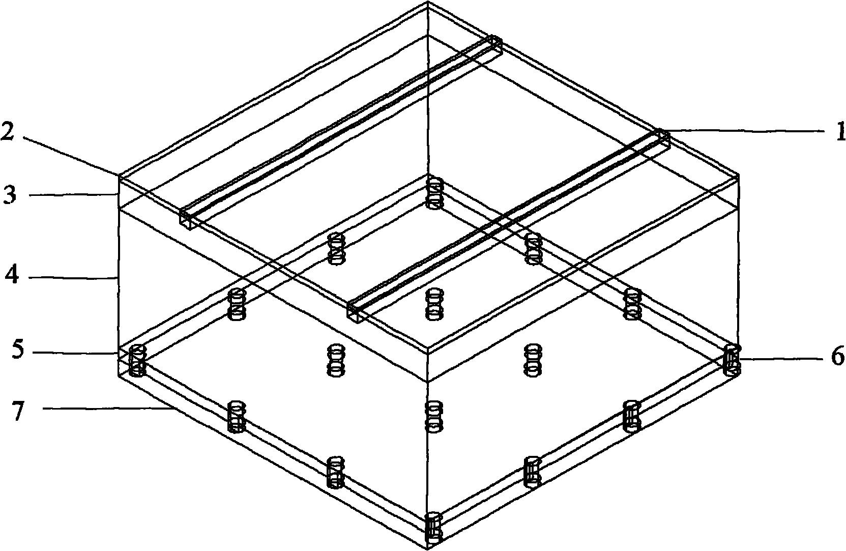
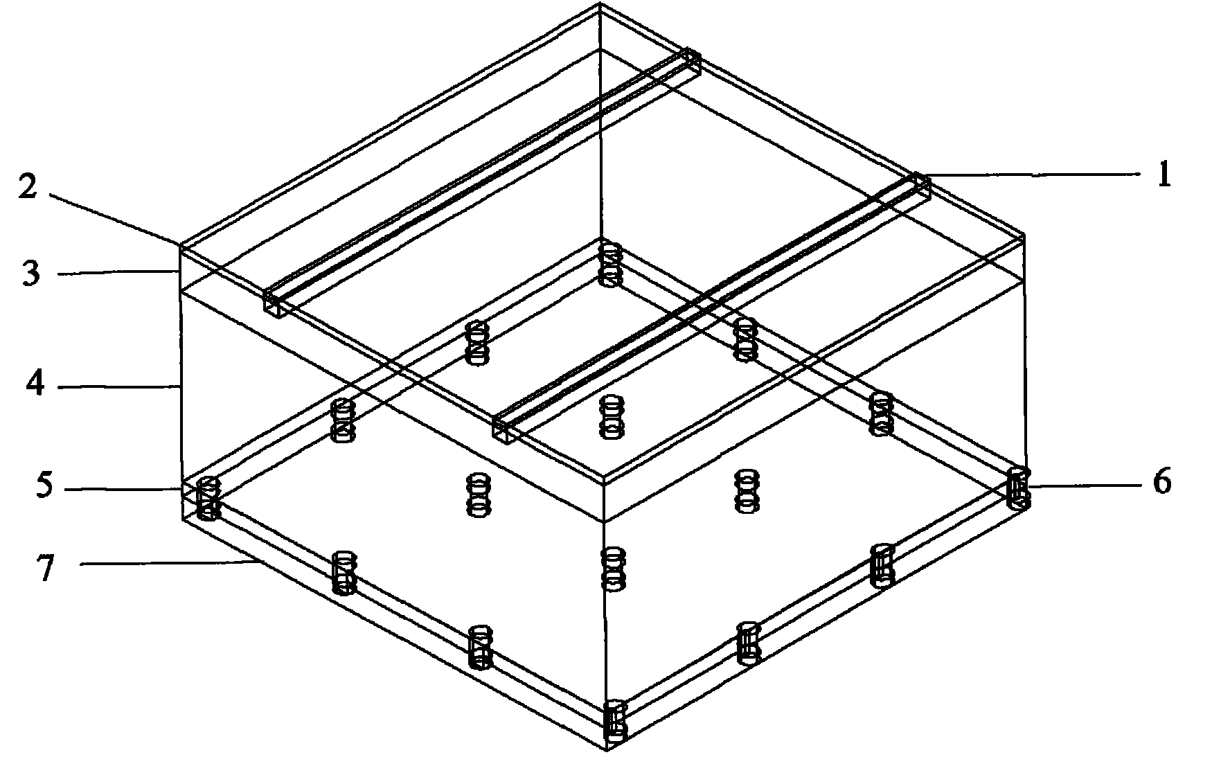
[0057] The preparation method of the N-type crystalline silicon partial aluminum back-emitter solar cell provided in this example: Select an N-type silicon wafer and perform surface texturing first, then use phosphorus diffusion to form a front surface field, and remove the phosphorus formed during the diffusion After phosphosilicate glass, a passivation film is deposited on the front surface, and then the silicon wafer is chemically polished on the back to remove the N+ layer formed on the back when phosphorus is diffused, and then the passivation film is deposited on the back, the back is partially opened or grooved, and the back wire Screen-print aluminum layer or silver-aluminum layer, then print silver paste on the front surface, and finally sinter once to form the ohmic contact between the local P+ layer on the back and the front and rear surface electrodes.

Embodiment 2

[0059] The preparation method of the N-type crystalline silicon partial aluminum back-emitter solar cell provided in this embodiment includes the following steps:

[0060] (1) Select N-type silicon wafers for surface texturing

[0061] For N-type monocrystalline silicon wafers, surface texturing is carried out at a temperature of 75-90°C in 0.5-5% by weight sodium hydroxide deionized aqueous solution; for N-type polycrystalline silicon wafers , in a mixed solution with a volume ratio of nitric acid, hydrofluoric acid and deionized water of 1 to 2:0.5 to 1:1, surface texturing under the condition of 5 to 15°C;

[0062] (2) Phosphorus diffusion forms the front surface field

[0063] The textured silicon wafer is diffused in a tubular double-sided manner using a phosphorus oxychloride liquid source to form a front surface field;

[0064] (3) Removal of phosphosilicate glass

[0065] After the phosphorus is diffused, the silicon wafer is immersed in hydrofluoric acid with a vol...

Embodiment 3

[0087] The preparation method of the N-type crystalline silicon partial aluminum back-emitter solar cell provided in this embodiment includes the following steps:

[0088] (1) Surface texturing

[0089] For (100) single-crystal N-type silicon wafers, use sodium hydroxide deionized aqueous solution containing 5 to 10% isopropanol or alcohol by volume to carry out single-sided etching under heating conditions (two pieces parallel to each other) insert together in the flower basket groove), make positive pyramid light-trapping structure, the weight percent content of above-mentioned sodium hydroxide aqueous solution is 0.5~5%, heating temperature is 75~90 ℃, the silicon wafer after the surface texturing is 10 % dilute hydrochloric acid for 2 minutes, rinse with deionized water, and set aside;

[0090] For polycrystalline N-type silicon wafers, use a mixed solution of nitric acid, hydrofluoric acid and deionized water with a volume ratio of 1 to 2:0.5 to 1:1 to react at 5 to 15°C...


PUM

PropertyMeasurementUnit
depthaaaaaaaaaa

Abstract

The invention provides a method for preparing an N-type crystalline silicon solar cell with aluminum-based local emitters on the back side. The method comprises the following steps: firstly, selecting N-type silicon wafers to carry out the surface-textured etching process; further forming a front surface field through phosphorous diffusion; depositing a passivating film on the front surface after the phosphorosilicate glass is formed during the removal of diffused phosphorous; carrying out the back-side chemical polishing process on the silicon wafers to remove the N+ layer formed on the back side during the phosphorous diffusion; then, sequentially printing an aluminum layer or a silver-aluminum layer through the passivating film deposited on the back side, local holes or grooves on the back side and screens on the back side; then, printing silver paste on the front surface; and finally, carrying out the one-step sintering process to form a local P+ layer on the back side and allowing the P+ layer to coming into ohmic contact with the electrodes on the front and back surfaces. By using the N-type substrate, forming local aluminum-based P-N junctions on the back side and further using the back-side chemical polishing process to remove the edge junctions, the invention can substitute for the conventional stacking-type plasma etching process, simplify the technological procedures and further bring a series of performance improvement to cells.

Description

technical field [0001] The invention belongs to the technical field of solar cells, and in particular relates to a preparation method of an N-type crystalline silicon partial aluminum back emitter solar cell. Background technique [0002] With the decrease of fossil energy and the resulting deterioration of the ecological environment, people are turning their attention from traditional fossil energy to new green energy. The most direct way for humans to obtain energy is to use solar energy, and solar cells are one of the most effective ways to convert solar energy into electrical energy. In recent years, the world output of solar cells has grown at an annual rate of 30-40%, making it one of the fastest-growing industries in the market. [0003] At present, crystalline silicon solar cells occupy a dominant position in the market. The vast majority of crystalline silicon production lines use boron-doped P-type crystalline silicon to make solar cell designs. The basic process...

Claims


Application Information

Patent Timeline
Patent Type & Authority Applications(China)
IPC IPC(8): H01L31/18
CPCY02P70/50
Inventor 金井升尹海鹏朱生宾何胜单伟
Owner JA YANGZHOU SOLAR PHOTOVOLTAIC ENG
Why Eureka
Try Eureka