Monomer charging and discharging tail balancing module and battery pack balancing protection management system thereof
A technology for equalizing modules and battery packs, applied to battery circuit devices, current collectors, electric vehicles, etc., can solve problems such as long paths, low efficiency, and large number of switch tubes, and achieve the effect of simple circuits
- Summary
- Abstract
- Description
- Claims
- Application Information
AI Technical Summary
Problems solved by technology
Method used
Image
Examples
Embodiment 1
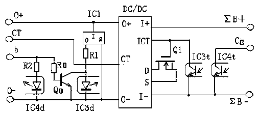
[0049] see figure 1 , Embodiment 1 of the present invention consists of DC voltage conversion controller DC / DC, first voltage detector IC1, first photocoupler IC3 (including input light-emitting diode IC3d and output phototransistor IC3t), second photocoupler IC4 ( Contains input light-emitting diode IC4d and output phototransistor IC4t), field effect transistor Q1, transistor Q0, first resistor R0, second resistor R1, and third resistor R2. These components are welded (or bonded or integrated) in the same package (or printed circuit board) to form a modular structure. It is set with: output positive contact 'O+', output negative contact 'O - ’, input positive contact’ ∑B+’ , input negative contact' ΣB-' , secondary control contact 'CT', equalization input contact 'b', charging control contact 'Cg'.
[0050] The DC / DC primary and secondary isolation of the DC voltage conversion controller is provided with an input positive pin 'I+' and an input negative pin 'I' - ’, outp...
Embodiment 2
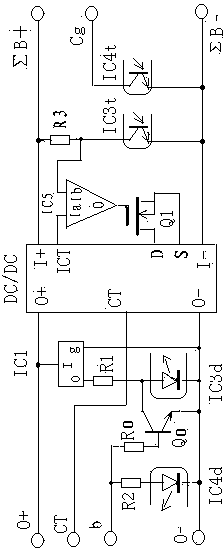
[0069] see figure 2 , the present invention can also set the AND gate circuit IC5 and the fourth resistor R3 on the basis of the first embodiment. The output pin 'O' of the AND gate circuit IC5 is connected to the gate of the field effect transistor Q1, and the first input pin 'Ia' of the AND gate circuit IC5 is connected to the primary control pin 'ICT' of the DC voltage conversion controller DC / DC, and the AND gate circuit The second input pin 'Ib' of IC5 is connected to the collector of the output phototransistor IC3t of the first photocoupler IC3, and the fourth resistor R3 is connected to the DC / DC input positive pin 'I+' of the DC voltage conversion controller and the first photocoupler The output of IC3 is between the collectors of phototransistor IC3t.
[0070] Adding the AND circuit IC5 and the fourth resistor R3 can reduce the driving current of the first photocoupler IC3 to the μA level, which means that the current consumption of the battery pack by the balanced ...
Embodiment 3
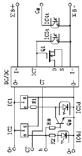
[0072] see image 3 , the basic principle structure of embodiment 3 of the present invention is the same as embodiment 1, and the difference is that embodiment 3 is formed after embodiment 1 (replacing embodiment 1 with embodiment 2. Another embodiment 3 is also established, for simplicity, no drawing ) on the basis of setting the second voltage detector IC2, the second voltage detector IC2 is used to detect the charging equalization voltage, and has an input pin 'I', an output pin 'O', and a common pin 'g' on it; the second voltage detector The input pin 'I' of IC2 is connected to the output positive contact 'O+' of the single charge-discharge tail-compensation equalization module, and its output pin 'O' is connected to the input light-emitting diode IC4d of the second photocoupler IC4 through the third resistor R2. The first resistor R0 is connected to the base of the triode Q0, and its common pin 'g' is connected to the output negative contact of the single charge and disch...
PUM
 Abstract
Description
Claims
Application Information


