Method for preparing graphene
A graphene and carbon source technology, applied in the field of graphene preparation on non-metallic materials, can solve the problems of difficult and weak adhesion, and achieve the effect of simple preparation process and convenient liquid phase processing
- Summary
- Abstract
- Description
- Claims
- Application Information
AI Technical Summary
Problems solved by technology
Method used
Image
Examples
Embodiment 1
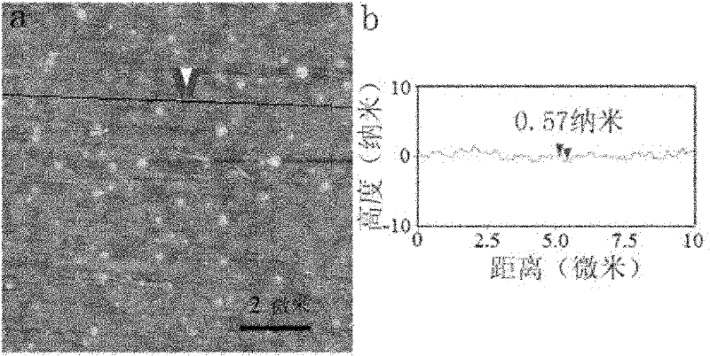
[0035] Embodiment 1, prepare graphene sheet on quartz substrate
[0036] 1) Clean the quartz growth substrate:
[0037] The quartz plate was ultrasonically cleaned with detergent, water, deionized water, acetone and ethanol for 5 minutes each, and then dried;
[0038] 2) Put the processed quartz sheet in step 1) into the quartz tube of the tube furnace, evacuate to reduce the air pressure in the tube to below 10 pascals, feed hydrogen to normal pressure, and repeatedly remove the air in the tube three times, and control the hydrogen flow rate to 50 sccm , heating up, when the temperature rises to 1100°C, continue to keep at constant temperature for 10 minutes;
[0039] 3) Growing graphene:
[0040] Maintain the temperature in the tube furnace quartz tube in step 2) to be 1100° C., the methane and the hydrogen of 50 sccm that feed flow are 12.5 sccm, at 1.01 × 10 5 After growing under Pascal pressure for 1 hour, turn off the methane as the carbon source, and cool down to roo...
Embodiment 2
[0042] Embodiment 2, prepare graphene film on quartz substrate
[0043] According to the same method as in Example 1, only the growth time in step 2) was extended to 5 hours.
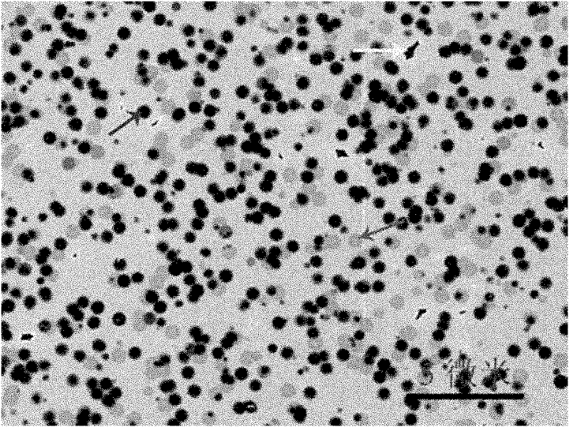
[0044] figure 2 It is a scanning electron microscope photo of a graphene film. The scanning electron microscope is a field emission scanning electron microscope S-4800. The accelerating voltage is 1kV. The area indicated by the green arrow is a single layer, the area indicated by the red arrow is a double layer, and the area indicated by the blue arrow It is a small number of layers or folds, and the area indicated by the yellow arrow is the base. Among them, the area of the single layer area is 60%, and the thickness is 0.95 nanometers, and the area of the double layer area is 15%. ) is 25% of the area.
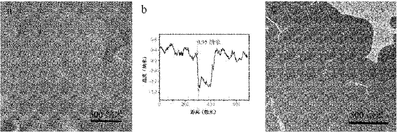
[0045] image 3 It is the atomic force microscope photo of the graphene film, where a is the height map, b is the height profile along the straight line in the picture a, and c is the phase di...
Embodiment 3
[0049] Embodiment 3, prepare graphene sheet on silicon wafer with silicon dioxide coating
[0050] According to the same method as in Example 1, only the quartz wafer used in steps 1) and 2) is replaced with a silicon wafer with a thickness of 300 nanometers of silicon dioxide coating as the growth substrate, and the growth time is replaced by 30 minutes, 1 hour, 1.5 hours and 2 hours, the graphene sheets provided by the present invention were obtained.
[0051] Figure 8 It is a scanning electron microscope photo of a graphene sheet grown on a silicon wafer with a silicon dioxide coating for 1.5 hours. The scanning electron microscope is a field emission scanning electron microscope S-4300, and the accelerating voltage is 15kV. It can be seen from the figure that the graphene sheet It is a circular structure with a diameter of 200-300 nanometers, wherein more than 96% of the graphene sheet is a single layer, and the rest are double layers.
[0052] Figure 9 It is an atomi...
PUM
| Property | Measurement | Unit |
|---|---|---|
| Thickness | aaaaa | aaaaa |
| Diffraction angle | aaaaa | aaaaa |
| Thickness | aaaaa | aaaaa |
Abstract
Description
Claims
Application Information


