
Hot air speed and air direction sensor based on thinning process and manufacturing method thereof

A wind speed, direction and sensor technology, which is applied in the manufacture of semiconductor/solid-state devices, the use of thermal variables to measure fluid velocity, instruments, etc. It can solve the problems of high power consumption, silicon wafer pollution and damage of the sensor system, and reduce the effect of lateral heat conduction. , the effect of isolating lateral heat conduction and reducing heat capacity

Inactive Publication Date: 2012-12-19
SOUTHEAST UNIV
View PDF0 Cites 0 Cited by
  • Summary
  • Abstract
  • Description
  • Claims
  • Application Information

AI Technical Summary

Problems solved by technology

As a result, silicon wafers are easily subject to various contaminations, resulting in unstable performance and even damage.
If a ceramic substrate with high thermal conductivity is used, and the silicon chip of the sensor is packaged by flip-chip packaging or thermally conductive adhesive, the above contradictions can be better avoided, but the heat generated by the sensor after packaging is extremely large. Part of it is dissipated from the silicon-based substrate in the form of heat conduction, and only a small part is heat-exchanged with the outside air through the ceramic, which greatly reduces the amplitude of the output sensitive signal, and the sensitive signal can be improved by increasing the power consumption of the sensor. amplitude, but it causes a large power consumption of the entire sensor system

Method used


Image

  • Hot air speed and air direction sensor based on thinning process and manufacturing method thereof
  • Hot air speed and air direction sensor based on thinning process and manufacturing method thereof
  • Hot air speed and air direction sensor based on thinning process and manufacturing method thereof

Examples


Embodiment 1

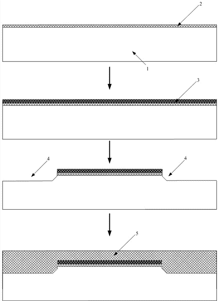
[0047] A preparation method of a thermal wind speed and direction sensor based on a thinning process is as follows:

[0048] The first step, the preparation of the silicon chip

[0049] Step 1, thermally growing a first thermal oxide layer 2 on the surface of the silicon chip 1;

[0050] Step 2, chemical vapor deposition of a silicon nitride layer 3 on the first thermal oxide layer 2;

[0051] Step 3, using RIE technology to etch the silicon chip 1 to define the active region 4;

[0052] Step 4, chemical vapor deposition of the second oxide layer 5;

[0053] Step 5, using CMP technology to polish the silicon chip 1;

[0054] Step 6, removing the silicon nitride layer 3 by wet etching, and preparing the field oxide layer 6;

[0055] Step 7, phosphorus ion implantation, preparing N well 7;

[0056] Step 8, thermally growing the gate oxide layer 8;

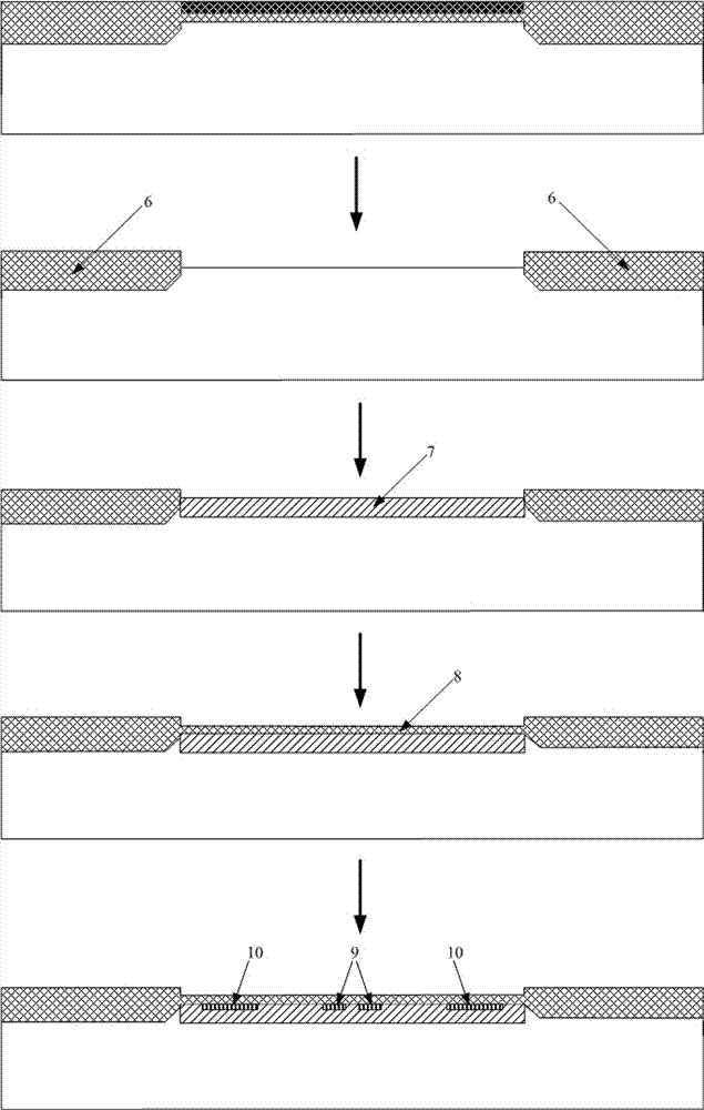
[0057] Step 9, boron ion implantation, preparing the heating element 9 and one end 10 of the heat sensing temperature measuri...

Embodiment 2

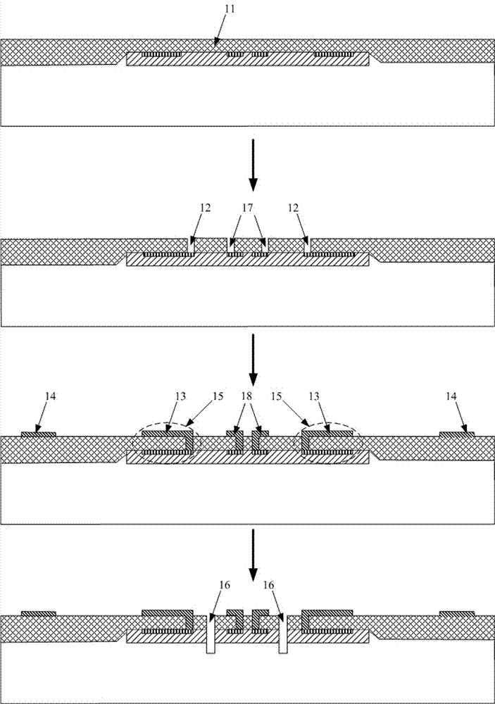
[0073] A thermal wind speed and direction sensor based on a thinning process is characterized in that it includes a thinned silicon chip 21, the back side of the thinned silicon chip 21 is connected with a ceramic substrate 23 through a thermally conductive glue 22, and the thinned silicon chip 21 is connected to a ceramic substrate 23. An N well 7 is provided on the front, an oxide layer 11 is provided on the N well 7, and 4 diffused resistance heating elements 9 and 4 heat sensing temperature measuring elements 15 are arranged in the middle of the N well 7. The temperature element 15 is a thermocouple temperature measuring element and is distributed around the four diffused resistance heating elements 9, and an electric lead-out pad 14 is provided on the edge area of ​​the oxide layer 11, and the electric lead-out pad 18 of the four diffused resistance heating elements 9 and the electric lead-out pads 13 of the four heat-sensing temperature-measuring elements 15 are respectiv...


PUM


Abstract

The invention provides a wafer level packaged hot air speed and air direction sensor realized by adopting a silicon substrate thinning process technology and a manufacturing method thereof. In a sensor chip, a heating element and a heat-sensitive temperature measuring element are manufactured by adopting a CMOS (Complementary Metal-Oxide-Semiconductor Transistor) process; a heat insulation groovewith the depth of 50 microns is formed between the heating element and the heat-sensitive temperature measuring element by adopting a dry etching process, so that transverse heat conduction effects between the heating element and the heat-sensitive temperature measuring element are reduced; a silicon substrate of a sensing chip is thinned by using a thinning process until the thickness of the silicon substrate is 80-100 microns, so that the heat conduction and the heat capacity of the substrate of the chip are lowered; and a ceramic substrate is attached to the back face of a thinned silicon chip to protect the silicon chip and sense the changes of the air speed and the air direction of the ambient temperature. By adopting the air speed and air direction sensor, wafer package is realized,the heat conduction loss of the silicon substrate and the heat capacity of the sensor chip are greatly lowered, and a large output signal and shorter response time can be obtained under low power consumption.

Description

technical field [0001] The invention relates to a wafer-level packaged thermal wind speed and direction sensor realized by silicon substrate thinning process technology. The sensor chip is prepared by standard CMOS integrated circuit technology, and especially relates to a low-power integrated wind speed sensor based on ceramic packaging. Wind direction sensor and preparation method thereof. Background technique [0002] In the design of CMOS integrated wind speed and direction sensors, packaging has always been a technical bottleneck hindering its development. On the one hand, the encapsulation material is required to have good thermal conductivity and to protect the sensor, and the impact of the encapsulation material on the sensitivity, reliability and price of the sensor needs to be considered in the design, which limits the sensor’s own encapsulation. Design freedom. On the other hand, the thermal flow sensor requires the sensitive part of the sensor to be exposed to ...

Claims


Application Information

Patent Timeline
Patent Type & Authority Patents(China)
IPC IPC(8): G01P5/10G01P13/02H01L21/822
Inventor 董自强黄庆安秦明
Owner SOUTHEAST UNIV
Learn More