Graded porous nano alumina/gold composite film electrode and preparation method thereof

A technology of nano-alumina and composite thin films, applied in the direction of material electrochemical variables, metal material coating technology, ion implantation plating, etc., can solve the problems of high brittleness of nano-porous AAO film, difficult electrode surface, difficult to handle, etc., to achieve The effect of good detection sensitivity, high electrocatalytic activity, and high electron transfer efficiency

Inactive Publication Date: 2011-09-14
HEFEI INSTITUTES OF PHYSICAL SCIENCE - CHINESE ACAD OF SCI
View PDF3 Cites 11 Cited by
  • Summary
  • Abstract
  • Description
  • Claims
  • Application Information

AI Technical Summary

Problems solved by technology

However, due to the high brittleness of the nanoporous AAO film, it is difficult to handle, making it difficult to apply it to the modification of the electrode surface on a large scale.

Method used


Image

  • Graded porous nano alumina/gold composite film electrode and preparation method thereof
  • Graded porous nano alumina/gold composite film electrode and preparation method thereof
  • Graded porous nano alumina/gold composite film electrode and preparation method thereof

Examples


Embodiment 1

[0016] 1. Preparation of multilayer composite films

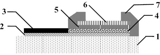
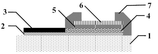
[0017] a. Use quartz as the insulating substrate. After thorough cleaning, dry it with nitrogen gas, and use magnetron sputtering to deposit the first bonding layer titanium layer on the insulating substrate with a thickness of 50 nm;

[0018] b. Using magnetron sputtering, a gold layer is deposited on the surface of the titanium layer of the first bonding layer, with a thickness of 120 nm;

[0019] c. Using magnetron sputtering, deposit a quasi-second bonding layer titanium layer at one end of the surface of the gold layer 7, with a thickness of 30 nm;

[0020] d. Depositing an aluminum layer with a thickness of 1000 nm on the quasi-second bonding layer titanium by thermal evaporation;

[0021] e. Using magnetron sputtering, deposit a silicon dioxide layer on the edge of the composite film with a thickness of 1300 nm;

[0022] 2. Anodizing multilayer films

[0023] f. Using an oxalic acid solution with a concentration...

Embodiment 2

[0031] 1. Preparation of multilayer composite films:

[0032] a. Use glass as the insulating substrate. After thorough cleaning, dry it with nitrogen gas, and use magnetron sputtering to deposit the first bonding layer of tantalum on the insulating substrate with a thickness of 80nm;

[0033] b. Using magnetron sputtering, a gold layer is deposited on the surface of the tantalum layer of the first bonding layer, with a thickness of 180nm;

[0034] c. Using magnetron sputtering, deposit a quasi-second bonding layer tantalum layer at one end of the gold layer surface, with a thickness of 40nm;

[0035] d, using thermal evaporation to deposit an aluminum layer on the quasi-second bonding layer tantalum layer, with a thickness of 2500nm;

[0036] e. Using magnetron sputtering, deposit a silicon dioxide insulating layer on the edge of the composite film layer, with a thickness of 2900 nm;

[0037] 2. Anodizing multilayer films

[0038] f. Using a phosphoric acid solution with ...

Embodiment 3

[0043] 1. Preparation of multilayer composite films:

[0044] a. Using a silicon wafer with silicon dioxide as the insulating substrate, after thorough cleaning, dry it with nitrogen, and use magnetron sputtering to deposit the first bonding layer of niobium on the insulating substrate with a thickness of 5 nm;

[0045] b. Using magnetron sputtering, a gold layer is deposited on the surface of the niobium layer of the first bonding layer, with a thickness of 80 nm;

[0046] c. Using magnetron sputtering, deposit a quasi-second bonding layer niobium layer at one end of the gold layer surface, with a thickness of 5 nm;

[0047] d. Depositing an aluminum layer with a thickness of 300 nm on the quasi-second bonding layer by magnetron sputtering;

[0048] e. Spin-coating process is used to cover SU-8 layer along the edge of the composite film layer, with a thickness of 400 nm;

[0049] 2. Anodizing multilayer films

[0050] d. Using a sulfuric acid solution with a concentratio...


PUM

PropertyMeasurementUnit
thicknessaaaaaaaaaa
thicknessaaaaaaaaaa
thicknessaaaaaaaaaa

Abstract

The invention relates to a composite film electrode and a preparation method thereof. The electrode is a graded porous nano composite film which is composed of an insulating substrate, a first binding layer, a conductive gold layer, a second binding layer and a modified aluminum layer, wherein small holes with a hole diameter of 2-20 nm are uniformly distributed on the conductive gold layer according to a distribution density of 1010/cm2-1012/cm2, and the small holes with the hole diameter of 20-400 nm are uniformly distributed on the second binding layer and the modified material layer according to the distribution density of 109/cm2-1012/cm2; and the preparation method of the electrode comprises the following steps of: firstly, preparing a multi-layer composite film on the insulating substrate, then, performing anodizing and hole enlargement on the multi-layer composite film to implement that an aluminum layer becomes a porous alumina layer, a gold layer becomes a nano porous structure, the second binding layer becomes a porous oxide of tantalum, niobium or titanium, and cleaning and drying the multi-layer composite film to get a finished product of the graded porous nano alumina/gold composite film electrode. The graded porous nano alumina/gold composite film electrode has high in electroanalytical activity and the dual advantages of a nano porous gold and a porous anodizedaluminum; and the preparation method is simple and reliable, solves the defect of inconvenience in operation caused by high brittleness of an AAO, and fits for mass production.

Description

technical field [0001] The invention relates to a composite thin film electrode and a preparation method thereof, in particular to an alumina / gold composite thin film electrode with a hierarchical porous nanostructure and a preparation method thereof. Background technique [0002] Nanostructured materials have a large specific surface area, and there are a large number of active centers such as dangling bonds and surface defects on the surface. Designing and modifying traditional electrodes based on nanostructures to improve the sensitivity, reliability and stability of electrochemical sensors has attracted more and more attention. [0003] Gold electrodes are widely used in electrochemical analysis as a traditional electrode material. Compared with the traditional gold electrode, the nanostructured gold electrode has a large specific surface area, and there are a large number of active centers such as dangling bonds and surface defects on the surface, which greatly impro...

Claims


Application Information

Patent Timeline
Patent Type & Authority Applications(China)
IPC IPC(8): G01N27/30C23C14/14C23C14/58
Inventor 林新华陈丽娟李加伟唐敏
Owner HEFEI INSTITUTES OF PHYSICAL SCIENCE - CHINESE ACAD OF SCI
Why Eureka
Try Eureka