Epitaxial structure of LED (light-emitting diode) with GaN (gallium nitride)-based vertical structure and manufacturing method thereof

An epitaxial structure and vertical structure technology, applied in electrical components, circuits, semiconductor devices, etc., can solve problems such as poor heat dissipation effect, stress damage, current congestion, etc., achieve low equipment requirements, achieve low cost, solve the problem of current congestion and Effect

Inactive Publication Date: 2011-10-12
云峰
View PDF6 Cites 12 Cited by
  • Summary
  • Abstract
  • Description
  • Claims
  • Application Information

AI Technical Summary

Problems solved by technology

[0007] The purpose of the present invention is to provide a gallium nitride-based vertical structure LED epitaxial structure and manufacturing method to overcome the problems of current congestion, poor heat dissipation, and stress and damage during the stripping process in the prior art

Method used


Image

  • Epitaxial structure of LED (light-emitting diode) with GaN (gallium nitride)-based vertical structure and manufacturing method thereof
  • Epitaxial structure of LED (light-emitting diode) with GaN (gallium nitride)-based vertical structure and manufacturing method thereof
  • Epitaxial structure of LED (light-emitting diode) with GaN (gallium nitride)-based vertical structure and manufacturing method thereof

Examples


Embodiment 1

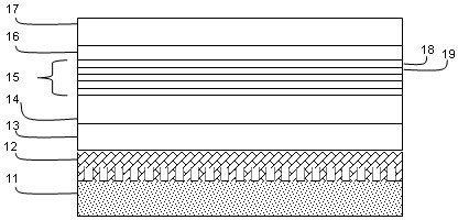
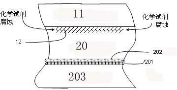
[0035] (1) Firstly, the ZnO buffer layer 12 is prepared on the epitaxial growth substrate 11, and the substrate: a patterned sapphire substrate is selected. see figure 2 , using a ZnO buffer growth structure on a patterned sapphire substrate see figure 2 . Define the pattern on the substrate by means of photolithography or mask, and form a submicron to several micron periodic surface convex-concave microstructure by wet etching or dry etching. The side of the microstructure is a quasi-nonpolar crystal plane or Non-polar crystal planes can also be curved. The molecular layer structure of ZnO is deposited on this substrate, and the deposition tool can be laser-assisted molecular beam epitaxy, laser sputtering, or oxide vapor phase epitaxy. The deposited ZnO film can be amorphous, polycrystalline, or single crystal. The thickness of ZnO is controlled at 0.1 micron to 100 micron.

[0036] (2) Continue to grow the extrinsically doped GaN buffer layer 13 on the grown ZnO thin f...

Embodiment 2

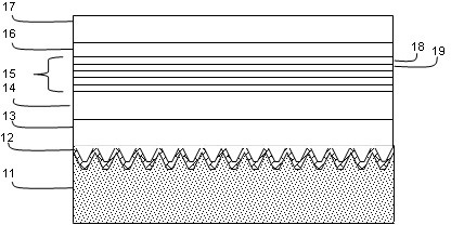
[0041] (1) Firstly, a ZnO buffer layer 12 is prepared on the epitaxial growth substrate 11, and the substrate: a planar sapphire substrate is selected. see figure 1 , first in the ZnO epitaxial technology using a three-dimensional preferential growth mode for self-organized growth, forming a high-density columnar ZnO nanowire structure with a diameter of several nanometers to submicrons on the substrate. The height of the nanowires is comparable to the pitch of the pillars. Then switch to the mode of lateral growth priority, grow a ZnO film with a thickness of 1 micron to 10 microns until the surface is flat, and all columnar ZnO structures are completely filled.

[0042] (2) Continue to grow the extrinsically doped GaN buffer layer 13 on the grown ZnO thin film substrate in metal organic vapor phase epitaxy (MOCVD) equipment. Firstly, the temperature of the reaction chamber is controlled below 500° C. to grow the low-temperature GaN buffer layer 13 , and at the same time, ...


PUM

PropertyMeasurementUnit
thicknessaaaaaaaaaa
thicknessaaaaaaaaaa

Abstract

The invention relates to an epitaxial structure of an LED (light-emitting diode) with a GaN (gallium nitride)-based vertical structure and a manufacturing method thereof. The manufacturing method adopts the following technical scheme which at least comprises the following steps: (1) manufacturing a ZnO buffer layer on an epitaxial growth substrate; (2) using MOCVD (metal-organic chemical vapor deposition) equipment to grow an extrinsic doped GaN buffer layer on the ZnO buffer layer substrate; (3) continuing to grow a high-temperature N-type Si-doped GaN layer, a periodical multilayer luminous zone-quantum well, an electronic barrier layer and a P-type Mg-doped GaN layer in the MOCVD equipment; and (4) carrying out charge carrier exciton on the Mg doped in the P-type GaN layer. The invention has the following advantages: a complicated ultraviolet laser peeling process and dear ultraviolet laser peeling equipment are not used when the substrate is peeled; in the manufacturing method, a damage-free mechanical-separation-free substrate peeling technology is adopted; the equipment is low in requirements; and the epitaxial wafers can be processed in batch.

Description

technical field [0001] The invention belongs to the technical field of semiconductor light-emitting diodes, and in particular relates to a gallium nitride-based vertical structure LED epitaxial structure and a manufacturing method. Background technique [0002] Semiconductor light-emitting diodes (Light Emitting Diode, hereinafter referred to as LED) based on compound semiconductor material gallium nitride (GaN) have been developing rapidly in technology and market since the early 1990s when blue light emitting light was practically realized. has also been greatly improved. [0003] The basis of the LED device is the semiconductor P-N junction, and the carrier recombination region composed of the quantum well multilayer structure between the P-N junctions, that is, the light-emitting region. The most commonly used epitaxial growth substrate is c-plane sapphire (Al2O3) single crystal substrate, and the most commonly used epitaxial tool is metal organic vapor phase epitaxy (M...

Claims


Application Information

Patent Timeline
Patent Type & Authority Applications(China)
IPC IPC(8): H01L33/00H01L33/02H01L33/06
Inventor 云峰
Owner 云峰
Why Eureka
Try Eureka