
An electrochemical method for the controllable preparation of silicon nanostructure materials

A structural material, silicon nanotechnology, applied in the direction of anodic oxidation, etc., to achieve the effect of easy separation or transfer, and easy operation

Inactive Publication Date: 2011-11-30
TECHNICAL INST OF PHYSICS & CHEMISTRY - CHINESE ACAD OF SCI
View PDF1 Cites 6 Cited by
  • Summary
  • Abstract
  • Description
  • Claims
  • Application Information

AI Technical Summary

Problems solved by technology

However, there is no report on the electrochemical reaction system in this respect

Method used


Image

  • An electrochemical method for the controllable preparation of silicon nanostructure materials
  • An electrochemical method for the controllable preparation of silicon nanostructure materials
  • An electrochemical method for the controllable preparation of silicon nanostructure materials

Examples


Embodiment 1

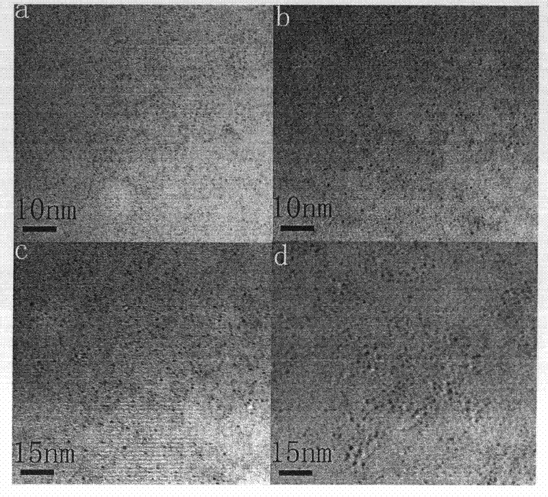
[0028] Embodiment 1, preparation particle diameter is the silicon quantum dot of 1-4nm

[0029] Mix ethanol solution with a mass concentration of 95%, hydrofluoric acid solution with a mass concentration of 20%, and hydrogen peroxide with a mass concentration of 30% in a volume ratio of 2:1:0.1, add phosphotungstic acid, and make the electrolyte The concentration of phosphotungstic acid in the mixture is 0.02 mg / mL, and after stirring evenly, an electrolyte solution for preparing silicon quantum dots is obtained.

[0030] P-type silicon wafer (conductivity 0.005-30Ω, reaction area 0.5-1cm 2) soaked in hydrofluoric acid with a mass concentration of 5% for 2-5 minutes, then rinsed with ethanol and distilled water in sequence, and then used as an anode, and a graphite rod as a cathode. Take 100ml of electrolytic solution and place it in a plastic electrolytic cell, and add 30 milliliters of cyclohexane into the electrolytic solution (reaction system) to form an organic solvent l...

Embodiment 2

[0031] Embodiment 2, preparation silicon nanoparticle

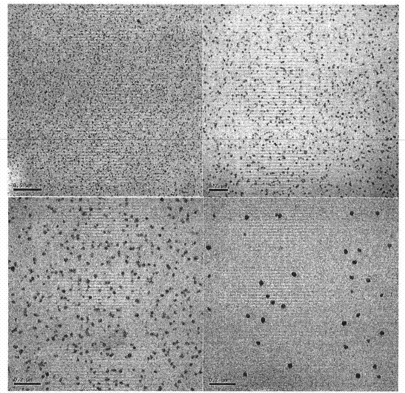
[0032] Mix 95% ethanol solution and 20% hydrofluoric acid solution according to the volume ratio of 1.5:1, add phosphomolybdic acid, so that the concentration of phosphomolybdic acid in the electrolyte is 0.03 mg / mL, and stir evenly to obtain Electrolyte for silicon quantum dots. Silicon wafer (conductivity 0.005-30Ω, reaction area 0.5-1cm 2 ) soaked in 5% hydrofluoric acid for 2-5 minutes, then rinsed with ethanol and distilled water successively, and then used as an anode, and a graphite rod as a cathode. Take 100ml of electrolytic solution and place it in a plastic electrolytic cell, and add 30ml of cyclohexane into the electrolytic solution to form an organic solvent liquid film above the electrolytic solution. at 15-20mA / cm 2 Under the current density of , the electrochemical oxidation reaction was carried out for 30 minutes, and silicon nanoparticles with a diameter of about 30 nanometers were obtained on the ano...

Embodiment 3

[0033] Embodiment 3, preparation silicon nanowire

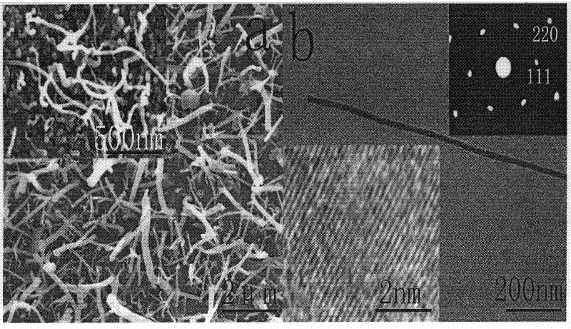
[0034] Prepare according to the method of Example 2, but change the current density of the reaction to 20-50mA / cm 2 , carry out the electrochemical redox reaction for 30-60 minutes, and obtain silicon nanowires with a diameter of about 30-80 nanometers on the anode silicon wafer. After the reaction, monodisperse silicon nanowires can be obtained by ultrasonically treating the anode silicon wafer in methanol or ethanol. image 3 . image 3 The inset in a is a partial enlargement, image 3 The upper inset in b is an electron diffraction pattern, and the lower inset is a high-resolution electron micrograph.


PUM

PropertyMeasurementUnit
concentrationaaaaaaaaaa
diameteraaaaaaaaaa
diameteraaaaaaaaaa

Abstract

The invention discloses a method for preparing a silicon nanostructure material or an array thereof. The method of the present invention comprises the following steps: using monocrystalline silicon as an anode and an inert electrode as a cathode, placing the anode and the cathode in an electrolytic solution, and adding a water-immiscible hydrocarbon solvent to the electrolytic solution; An electric current is applied to the anode to carry out an electrochemical oxidation reaction, and the silicon nanostructure material or its array is obtained after the reaction; wherein, the electrolyte is composed of a hydrofluoric acid solution with a mass concentration of 10-30%, an organic solvent and Catalyst composition; The organic solvent is methanol, ethanol or their mixture in any proportion, and the catalyst is polyacid compound, hydrogen peroxide or their mixture; The density of the water-immiscible hydrocarbon solvent is less than that of water density. By adjusting the type of catalyst and the current density of electrochemical reaction, the method can realize the controllable preparation of various silicon nanostructures and their arrays, and is a general preparation method for silicon nanostructures, which is simple and feasible.

Description

technical field [0001] The invention relates to an electrochemical method for controllable preparation of nanostructure materials. Background technique [0002] Silicon quantum dots and silicon nanostructures are considered to be the basic structural units of future electronic devices, new luminescent materials and catalytic materials, and have great potential application value in the fields of biosensing and biomedicine. Related research is of great significance in the field of nanoscience and technology. Due to the influence of quantum size effect and dielectric confinement effect, small-sized silicon nanoparticles have unique optoelectronic properties, which have shown attractive application prospects in the fields of light-emitting display, laser, lighting, solar cells and biomedicine. However, there are still many problems to be solved in the current research in this field, among which the most prominent is the poor control and repeatability of the preparation of silic...

Claims


Application Information

Patent Timeline
Patent Type & Authority Applications(China)
IPC IPC(8): C25D11/02
Inventor 康振辉刘阳张晓宏李述汤
Owner TECHNICAL INST OF PHYSICS & CHEMISTRY - CHINESE ACAD OF SCI
Learn More