

Preparation method of silicon quantum dot doped nano titanium dioxide film composite material
A nano-titanium dioxide and thin-film composite material technology, applied in metal material coating process, ion implantation plating, coating and other directions, can solve the problem of not forming silicon quantum dots, and achieve the effect of overcoming easy agglomeration
- Summary
- Abstract
- Description
- Claims
- Application Information
AI Technical Summary
Problems solved by technology
Method used
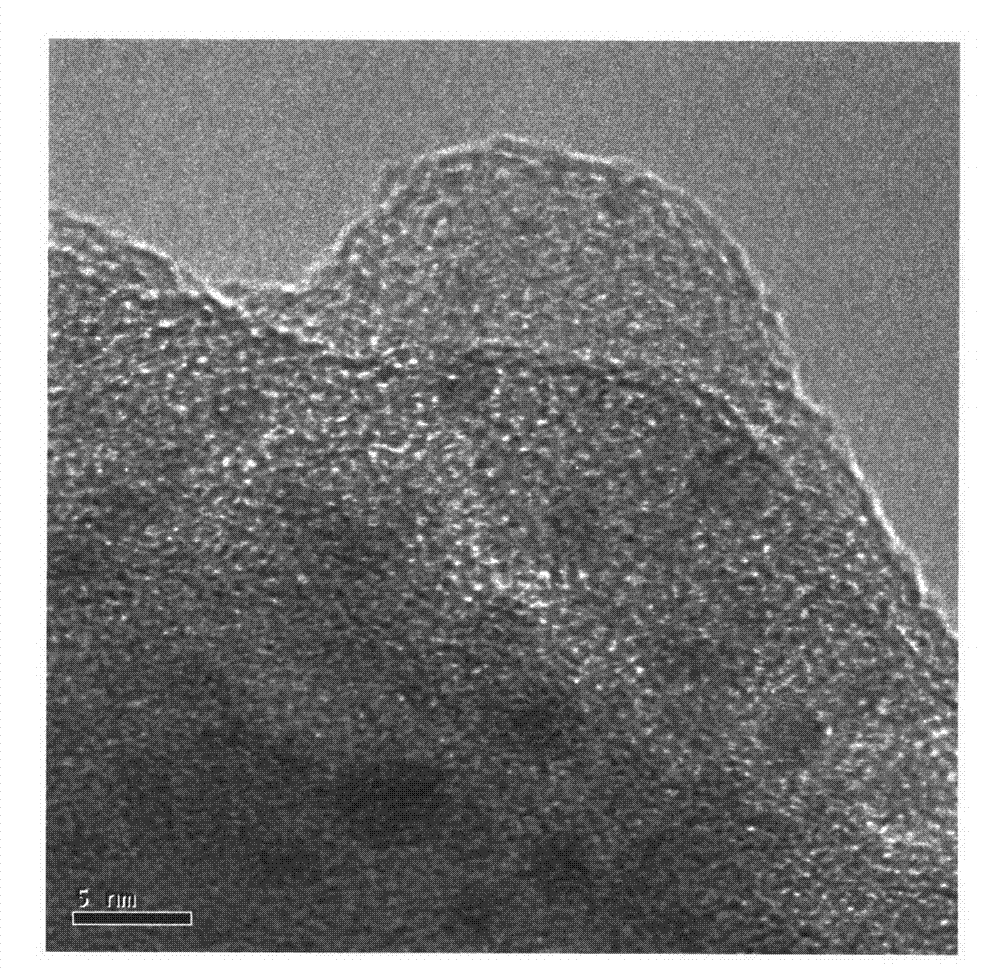
Image

Examples
example 1
[0016] The equipment used in the film preparation process of the present invention is the IBAD-600 multifunctional ion implantation and ion beam sputtering system;
[0017] The equipment used in the ion implantation preparation process is FM2000 nanometer multi-layer film composite machine.
[0018] The process of preparing nano-titanium dioxide film composite material doped with silicon quantum dots is as follows: soak a 2cm×2cm square quartz substrate in acetone solution and clean it for 15 minutes, then ultrasonically clean it with absolute ethanol for 10 minutes, and finally clean it with a large amount of deionized water; The surface of the titanium dioxide target material (10cm×10cm) with a mass purity of 99.99% was wiped clean with absolute ethanol. Then the cleaned quartz substrate and titanium dioxide were respectively fixed on the substrate and the target in the sputtering vacuum chamber, and vacuumed to make the background vacuum degree reach 8×10 -4 Pa, and then p...
example 2
[0020] The preparation process of the titanium dioxide film required for preparing the nano-titanium dioxide film composite material doped with silicon quantum dots is the same as that of Example 1.
[0021] Using ion implantation equipment, vacuumize to make the background vacuum degree reach 8.0×10 -4 Pa, when injecting, the environmental protection gas is high-purity argon, and the working vacuum is 2.0×10 -2 Pa, the substrate temperature is 25°C; then, the prepared titanium dioxide thin film is first implanted with an implant energy of 70keV and an implant dose of 1×10 16 cm -2 Perform silicon ion implantation for the first time, so that the implanted silicon ions are concentrated at the bottom of the titanium dioxide film; then the implantation energy is 50keV, and the implantation dose is 1×10 16 cm -2 Carry out the second ion implantation, so that the implanted silicon ions are concentrated in the middle; finally, at 30keV, the implantation dose is 1×10 16 cm -2 Th...
example 3
[0023] The preparation process of the titanium dioxide film required for preparing the nano-titanium dioxide film composite material doped with silicon quantum dots is the same as that of Example 1.
[0024] Using ion implantation equipment, vacuumize to make the background vacuum degree reach 9.0×10 -4 Pa, when injecting, the environmental protection gas is high-purity argon, and the working vacuum is 1.0×10 -2 Pa, the substrate temperature is 200°C; then, the prepared TiO2 thin film is first implanted with an implant energy of 60keV and an implant dose of 3×10 17 cm -2 Perform silicon ion implantation for the first time, so that the implanted silicon ions are concentrated at the bottom of the titanium dioxide film; then the implantation energy is 40keV, and the implantation dose is 3×10 17 cm -2 Perform the second ion implantation, so that the implanted silicon ions are concentrated in the middle; finally at 30keV, the implantation dose is 3×10 17 cm -2The third silicon...
PUM
| Property | Measurement | Unit |
|---|---|---|
| thickness | aaaaa | aaaaa |
Abstract
Description
Claims
Application Information